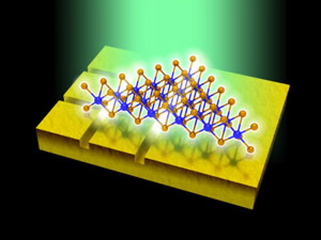
A*STAR researchers find tiny trenches patterned into a gold surface enhance photoluminescence efficiency. Reproduced from Ref. 1 and licensed under CC BY 4.0 © 2016 Z. Wang et al.
Future ultrathin solar cells and light sources could have their surfaces covered by tiny trenches, after A*STAR researchers found such structures enhance efficiency by four orders of magnitude.
Joel Yang from the A*STAR Institute of Materials Research and Engineering was part of an international collaboration that achieved a 20,000-fold increase in the photoluminescence of a one atom-thick layer of tungsten diselenide, by mounting it on a gold surface patterned with narrow trenches [1].
Tungsten diselenide is promising for ultra-sensitive, ultra-thin light sensors, solar cells and light-emitting diodes, because of its ability to absorb light and re-emit at a different frequency. However this effect only occurs for a single atom layer, so its efficiency is very low – most of the light passes straight through.
Yang’s inspiration was to mount the layer on a gold surface and trap the light energy at the interface of the two layers in the form of surface plasmons. To enhance the absorption of light, they added trenches to the gold layer under the tungsten diselenide.
“It was very surprising that such a large enhancement could be possible,” says Yang.
The key was matching the trench size to the energy so that the plasmons were trapped in the trenches through a resonant process known as the Purcell effect.
The team shone 633-nanometer light onto the sample and measured the output at 750 nanometers. They found 12 nm wide trenches in a grid pattern with spacing 200 nanometers gave the highest photoluminescence – 20,000 times more than a bare layer of tungsten diselenide.
To create the structure, the team etched a very flat silicon crystal to create a grid of ridges. Next they deposited a layer of gold onto the silicon and then peeled it off to reveal trenches where the ridges had been.
“The narrowness of the trenches and the flatness of the metal film is important,” Yang says. “Any roughness will interact detrimentally with the two-dimensional material.”
The gold was immersed in water and a film of tungsten diselenide floated on the water’s surface. The gold was then slowly raised out of the solution, emerging with the thin layer on top.
The simple structure has many advantages, says Yang. “The entire surface is exposed to the user, which makes it easy for further research, such as functionalizing the surface with chemicals or adding electrodes”.
It is also easier to manufacture than other plasmonic devices, which require a second layer above the thin layer, creating a sandwich.
The A*STAR-affiliated researchers contributing to this research are from the Institute of Materials Research and Engineering.


