Dr. Hyeon-Jun Lee (left) and Dr. Jun Seok Kim (right) at DGIST's Intelligent Devices and Systems Research Group
A research team of Intelligent Devices and Systems Research Group at DGIST has revealed the causes of structural disorder and defects of electrons due to fatigue accumulation occurring when oxide semiconductors are driven at high speed.
It is true that oxide semiconductors have superior conductivity compared to silicon semiconductors and are widely used in industry today because of their high conductivity at the nanometer level. Also, due to their high electron mobility and their ability to use existing semiconductor mass production processes, they are utilized in fields such as development systems for realizing artificial intelligence (AI) and attracting attention as a core material for next-generation display devices.
However, it has been difficult to commercialize oxide semiconductors because of various problems including fatigue accumulation phenomena that occur due to electrical signals.
In this study, the research team has found that asymmetric electron flow disturbance causes fatigue accumulation in electronic devices that use oxide semiconductors driven at high speed by demonstrating fatigue defects using high-frequency AC (Alternating Current) signal injection experiments and numerical calculations.
The researchers discovered the phenomenon of device failure due to fatigue accumulation by applying two methods simultaneously: a reliability evaluation method that injects AC signals similar to the signals applied in an integrated circuit in various frequencies and a method of evaluating the fatigue accumulation phenomenon in integrated devices.
In addition, the research team has proven that this fatigue accumulation phenomenon occurs in asymmetric local regions, and acts as an energy barrier to the flow of electrons that shortens the lifetime of the device by demonstrating by numerical analytic methods.
The fatigue defects phenomenon identified by the research team is closely linked to the reliability and lifetime of all electronic products operated by electronic signals. Therefore, the discovery is expected to lead to the development of core technologies that minimize errors in information processing and data transmission of electronic devices.
Dr. Lee stated “This research is significant and meaningful because it is the first in the world to identify the causes of fatigue defects that have been regarded as a major obstacle to the commercialization of oxide semiconductors.” He added “Through subsequent research and development, we will make efforts to develop next-generation intelligent electronic devices that do not suffer from fatigue defects and will try to speed up the commercialization of related technologies.”
This research outcome was published in the August and December 2017 editions of Scientific Reports, the sister journal of the globally renowned academic journal Nature.
For more information, please contact:
Dr. Hyeon-Jun Lee, Senior Researcher
Intelligent Devices and Systems Research Group
Daegu Gyeongbuk Institute of Science and Technology (DGIST)
E-mail: [email protected]
Journal Reference
Hyeon-Jun Lee, Sung Haeng Cho, Katsumi Abe, Myoung-Jae Lee, & Minkyung Jung, “Impact of transient currents caused by alternating drain stress in oxide semiconductors,” Scientific Reports August 2017.
https://www.nature.com/articles/s41598-017-10285-2
Hyeon-Jun Lee, Katsumi Abe, Jun Seo Kim, & Myoung-Jae Lee, “Electron-blocking by the potential barrier originated from the asymmetrical local density of state in the oxide semiconductor,” Scientific Reports December 2017.
https://www.nature.com/articles/s41598-017-18420-9
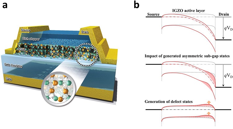
a) Schematic image and band state with defects in the degraded oxide semiconductor thin film transistors. (b) The broken bonds create many defect states on the IGZO (Indium Gallium Zinc Oxide) active layer at the drain side, and consequently impair the current capability of the distorted local host band structure.