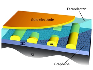
Schematic illustration of an improved graphene–ferroelectric FET with SiO2 basal layer.
A fundamental component of a field-effect transistor (FET) is the gate dielectric, which determines the number of charge carriers—electrons or electron vacancies—that can be injected into the active channel of the device. Graphene has recently become the focus of attention as a viable, high-performance replacement for silicon in FETs, and in recent studies on graphene-based FETs, scientists have investigated the use of thin films of a ferroelectric material for the gate dielectric. Such films offer several interesting advantages for use in graphene-based FETs: their strong electrical polarization makes it possible to introduce a much higher density of carriers than can be achieved using standard dielectrics, and they have remnant electric polarization—a property that could allow graphene–ferroelectric FETs to be used for nonvolatile memory by storing a certain level of carrier density in the absence of an electrical field.
Two collaborating teams from the A*STAR Institute of Materials Research and Engineering and the National University of Singapore, led by Kui Yao and Barbaros Özylmaz, respectively, previously demonstrated a basic graphene–ferroelectric memory device in which the polarization in the ferroelectric film was controlled by the electrical bias applied to the gate terminal. In that structure, a thin ferroelectric film was deposited on top of a graphene layer, where it injects charge carriers and thus modulates the resistance of the graphene. Unfortunately, however, the two distinct resistance states that could be read as an information bit could only be realized by polarizing and depolarizing the ferroelectric film, which presented problems due to the instability of the depolarization state.
Now, the two teams have collaborated to fabricate an improved device[1] that includes an additional silicon dioxide (SiO2) dielectric gate below the graphene layer (see image). The SiO2 gate, a long-standing component in traditional FETs, effectively provides a reference point from which to measure the effect of ferroelectric gating. By monitoring the resistance of the device as a function of the voltages applied to the top and bottom gates, the researchers developed a quantitative understanding of the performance and switching behavior of graphene–ferroelectric FETs. For use as a nonvolatile memory device, the SiO2 dielectric gate also simplifies bit writing by providing an additional background source of charge carriers, allowing the ferroelectric polarization to be switched between two stable states corresponding to two opposite polarization orientations.
The new device developed by the research team achieved impressive practical results, capable of symmetrical bit writing with a resistance ratio between the two resistance states of over 500% and reproducible nonvolatile switching over 100,000 cycles.
The A*STAR-affiliated researchers contributing to this research are from the Institute of Materials Research and Engineering