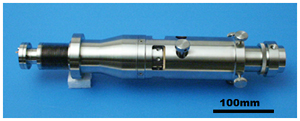
Fig. 1: Outlook of the SLEEM detector.
If a through-the-lens detector is applied, the pole piece nose of the objective lens can play the role of the anode. Primary electrons are retarded in the CL field and emitted electrons are collimated toward the optical axis and accelerated toward the detector. Important circumstance is that even the backscattered electrons (BSE) emitted under large angles with respect to the surface normal, which are abandoned in a standard SEM, are available now for the detection. This signal contribution has proven itself bearing enhanced crystallographic information.
Using the SLEEM offers several advantages. When lowering energy of the electron beam, the range of primary electrons shortens and the secondary electron (SE) yield grows. As a result, the beam-specimen interaction is more localized, charging artifacts drop off and the depth of radiation damage of the specimen decreases. The new designed detector by Institute of Scientific Instruments (See Fig. 1), Brno, Czech Republic is available to adopt for the conventional SEM like as Fig. 2. It is possible to obtain 15nm of resolution using 100eV electrons, although you usually need 10 keV for the same resolution. Fig. 3 shows a SLEEM image obtained by FESEM with SLEEM detector. Reacted products of MgAl2O4 on the surface of α-Al2O3 particles in Al-Mg-Si alloy are visible and their morphology has been also recognized as polygonal. The combination of high resolution SEM and SLEEM detector is really useful for the research of the surface science.
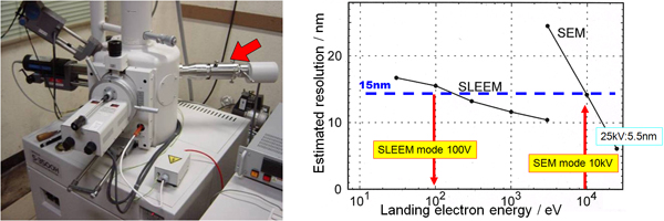
Fig. 2: Conventional SEM with SLEEM detector and its estimated resolution.
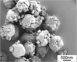
Fig. 3: SLEEM image for Alumina particle with reacted phase on their surface.