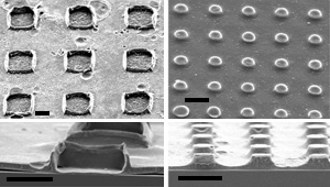
Scanning electron microscope images of (PDADMAC-PSS)10 films assembled on PMMA templates with ’microwells’ of 25 (left) and 7 (right) micrometers. Thinner films form inside larger microwells, and vice-versa. All scale bars: 10 μm.
Polymer films that undergo nanoscale structural transformations in response to external stimuli are key components of devices like biosensors and artificial membranes. One of the best materials for manufacturing such responsive materials is polyelectrolyte multilayers (PEMs) — polymer chains bearing charged units that can assemble layer-by-layer onto solid surfaces. Maxim Kiryukhin at the A*STAR Institute of Materials Research and Engineering and co-workers1 have now gained new insights into PEM growth which may enable construction of three-dimensional microstructures for on-demand drug delivery.
The standard method of producing PEMs involves repeatedly dipping a flat substrate into positively and negatively charged polyelectrolyte solutions. Although this approach can generate large-scale coatings with precise vertical thicknesses, it is far more challenging to achieve similar control at confined dimensions. Previous studies have shown that PEMs grown onto micro-sized surface templates have non-uniform thicknesses that could severely compromise device performance.
Kiryukhin and co-workers systematically investigated a PEM assembled from poly(diallyldimethylammonium chloride)/poly(sodium 4-styrenesulfonate), or PDADMAC–PSS, to help resolve this problem. Unlike other multilayers, the PDADMAC–PSS system can shift from a linear layer-by-layer growth mode to one with exponentially increasing film thickness, simply by increasing the ionic strength of the polyelectrolyte dipping solution. By exploring these two regimes on templates containing differently sized ‘microwells’, the team hoped to discover the critical factors needed to produce consistent microstructures.
First, the researchers imprinted an array of microwells ranging from 2 to 25 micrometers onto a sacrificial plastic template made of poly(methyl methacrylate), or PMMA, and then coated the surface with a PDADMAC–PSS multilayer film. After transferring the PEM onto a silicon support, they dissolved away the PMMA template. Depending on the microwell pattern, the polyelectrolyte concentration, and number of multilayers, this technique generated numerous structures including hollow microchambers and solid microstubs (see image).
The team found that in exponential growth modes, aggregation of PDADMAC chains produced variable template coatings; thicker films could form inside the microwells and vice-versa, depending on the particular template shape. Weak bonds between the PDADMAC aggregates gave these films gel-like mechanical properties. In linear growth modes, the solvated polyelectrolyte exists as isolated chains that coat the template evenly and make the microstructures rigid and glass-like. Stable hollow microchambers formed in this mode when the PEM film was thicker than 400 nanometers.
According to Kiryukhin, the highly ordered arrays of sealed microchambers produced with this method could allow programmed release of tiny ‘cargos’ from individual cavities — opportunities that the team are currently pursuing.
The A*STAR-affiliated researchers contributing to this research are from the Institute of Materials Research and Engineering