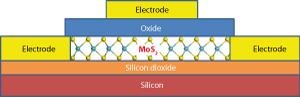
Transistors made of films of two-dimensional molybdenum disulfide (MoS2) could be integrated with other silicon electronics devices. © 2015 A*STAR Institute of Materials Research and Engineering
Two-dimensional materials have a whole host of exotic properties because they are just one atom thick. A*STAR researchers have now developed a method for creating large areas of atom-thin material for use in electronic devices [1].
Graphene, a single layer of carbon atoms arranged into a honeycomb-like pattern, is the most famous example of a two-dimensional material. It is stronger than steel, has excellent electrical properties, and could be used to make two-dimensional devices that are much smaller than those currently made from bulk or thin-film silicon. However, it is not a semiconductor. And so scientists are turning to other materials that have this essential property for creating transistors.
Shijie Wang from the A*STAR Institute of Materials Research and Engineering and his collaborators have now demonstrated a technique for creating a single atomic layer of molybdenum disulfide — a two-dimensional semiconductor.
Molybdenum disulfide belongs to a family of materials called transition-metal dichalcogenides. They have two chalcogenide atoms (such as sulfur, selenium or tellurium) for every transition-metal atom (molybdenum and tungsten are examples). These materials and their wide range of electrical properties provide an excellent platform material system for versatile electronics. But creating high-quality material over areas large enough for industrial-scale production is difficult.
“Traditional mechanical exfoliation methods for obtaining two-dimensional materials have limited usefulness in commercial applications, and all previous chemical methods are incompatible for integration with device fabrication,” says Wang. “Our technique is a one-step process that can grow good-quality monolayer films, or few layers of molybdenum disulfide films, at wafer scale on various substrates using magnetron sputtering.”
The team fired a beam of argon ions at a molybdenum target in a vacuum chamber. This ejected molybdenum atoms from the surface where they reacted with a nearby sulfur vapor. These atoms then assembled onto a heated substrate of either sapphire or silicon. The team found that they could grow monolayer, bilayer, trilayer or thicker samples by altering the power of the argon-ion beam or the deposition time.
They confirmed the quality of their material using a number of common characterization tools including Raman spectroscopy, atomic force microscopy, X-ray photoelectron spectroscopy and transmission electron microscopy. The researchers also demonstrated the excellent electrical properties of their molybdenum disulfide films by creating a working transistor (see image).
“Our next step in this work will focus on the application of this technique to synthesize other two-dimensional materials and integrate them with different materials for various device applications,” says Wang.
The A*STAR-affiliated researchers contributing to this research are from the Institute of Materials Research and Engineering. More information about the group’s research can be found at the Design and Growth webpage.
Reference
[1] Tao, J., Chai, J., Lu, X., Wong, L. M., Wong, T. I. et al. Growth of wafer-scale MoS2 monolayer by magnetron sputtering. Nanoscale 7, 2497–2503 (2015).