Complete control of light waves would allow the miniaturization of traditional optical components, such as lenses, polarizers or beam-splitters, to nanoscale sizes while dramatically increasing their performance and resolution.
Complete control of some of the key properties of light waves – namely their polarisation and phase – at the nanoscale is of major interest for light-based technologies such as display screens, and in energy harvesting and data transmission. It would allow, for example, the miniaturization of traditional optical components, such as lenses, polarizers or beam-splitters, to nanoscale sizes. At the same time, it could dramatically increase their performance and resolution.
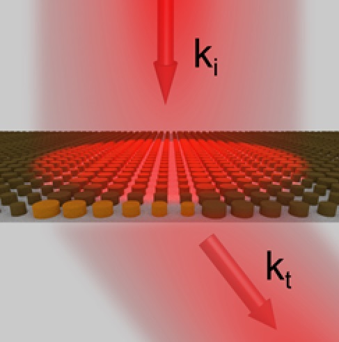
A novel approach to control the propagation of light at the nanoscale involves the use of so-called metasurfaces. A metasurface is a two-dimensional arrangement of nanosized particles called nanoantennae. Their geometries and material properties are cleverly designed to interact with light in a determined way. By engineering such metasurfaces, it is possible to modify the overall path of the light and, for example, make it bend or focus at a certain point of space, similar to what conventional prisms or lenses do. In the case of metasurfaces, this happens at distances that are 1,000 times smaller than the diameter of a human hair.
Researchers at the Agency for Science, Technology and Research (A*STAR) in Singapore have demonstrated that using silicon nanoparticles as nanoantennae, in place of metals used in previous research, allows full control of an incoming light beam while keeping it essentially transparent, allowing transmission rates above 85%. By controlling the spatial distribution of the silicon nanoparticles, they were able to bend a light beam with record efficiencies of about 50%: a level that could be further increased by optimising the system.
When metals were used to design nanoantennae, they caused strong reflections of light making them unsuitable for devices that transmit data. Heating induced in the metals also resulted in additional losses in the device, a serious drawback for real-world applications that require high efficiency. Silicon, as a semiconducting material, overcomes these issues, the A*STAR researchers found.
While the team’s future research will focus on creating switchable or reconfigurable devices, together with new materials in different spectral regions, the technological challenge will be to develop fully viable ultra-flat optical devices for commercial uses.
Did you know? The polarisation of light refers to the orientation of the electric field in a light wave, while the phase of light refers to the specific state of a light wave.
For further information contact:
Dr Arseniy Kuznetsov
Data Storage Institute
Agency for Science, Technology and Research, Singapore
E-mail: [email protected]