A research team, led by Professor Jun Hee Lee in the School of Energy and Chemical Engineering at UNIST has proposed a new physical phenomenon that promises enhanced storage capacity of a fingernail-sized memory chip by 1,000 times. This is expected to offer unexpected opportunities for ultimately-dense unit-cell-by-unit-cell ferroelectric switching devices directly integrable into silicon technology, according to the research team.
Ferroelectric random access memory (FeRAM or FRAM) stores information through the phenomenon of polarization, in which an electric dipole, like the N-S magnetic fields inside ferroelectrics, are aligned by an external electric field. FeRAM has emerged as the next-generation memory semiconductor to replace the existing DRAM or flash memories, as it is faster, uses less power, and even retains stored data after the power is turned off.
However, one major drawback of FeRAM is that it has limited storage capacity. And thus, in order to increase its storage capacity, it is necessary to integrate as many devices as possible by reducing the chip size. In the case of ferroelectrics, the reduction in physical dimension results in disappearance of the phenomenon of polarization that aids in storing information in ferroelectric materials. This is because the formation of ferroelectric domains, the tiny regions where the spontaneous polarization occurs, requires at least a group of thousands of atoms. Therefore, current research on FRAM technology focuses on reducing the domain size, while keeping the storage capacity.
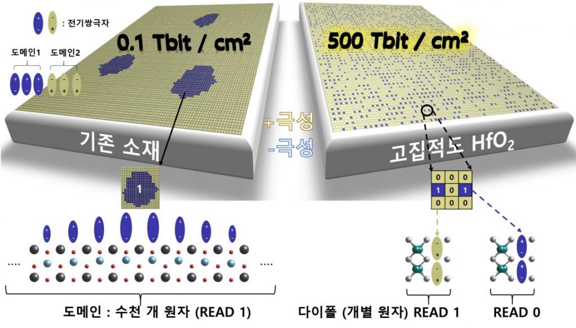
Figure 1. A schematic image comparing current (left) and new (right) FeRAMs.
Professor Lee and his research team discovered that by adding a drop of electrical charge to semiconductor material known as ferroelectric hafnium oxide (HfO2), it is possible to control four individual atoms to store 1 bit of data. This groundbreaking research has overturned the existing paradigm, which is capable of storing 1 bit of data in a group of thousands of atoms, at best. When properly applied, a semiconductor memory can store 500 Tbit/cm2, 1,000 times bigger storage than flash memory chips that are currently available.
“The new technology, enabling storing data in individual atoms is the highest-level storage technology that has been developed so far,” says Professor Lee. “As HfO2 is already compatible in Si-electronics, our discovery of independently switchable polar layers could provide opportunities to realize ultra-dense and low cost FeRAM or FeFET for memory or logic device applications.” He adds, “In addition, possibility of unit-cell-by-unit-cell dipolar control provides different opportunities for deterministic multilevel switching, ultimately down to the angstrom scale.”
This revolutionary discovery has been supported by Samsung Research Funding and Incubation Center of Samsung Electronics and thorugh the Future Materials Discovery program by the Ministry of Science and ICT (MSIT), as well as the Industrial Strategic Technology Development Program by the Creative Materials Discovery program by the Ministry of Trade, Industry Energy (MOTIE). The findings of this research have been published in Science on July 2, 2020.
Advertisement