

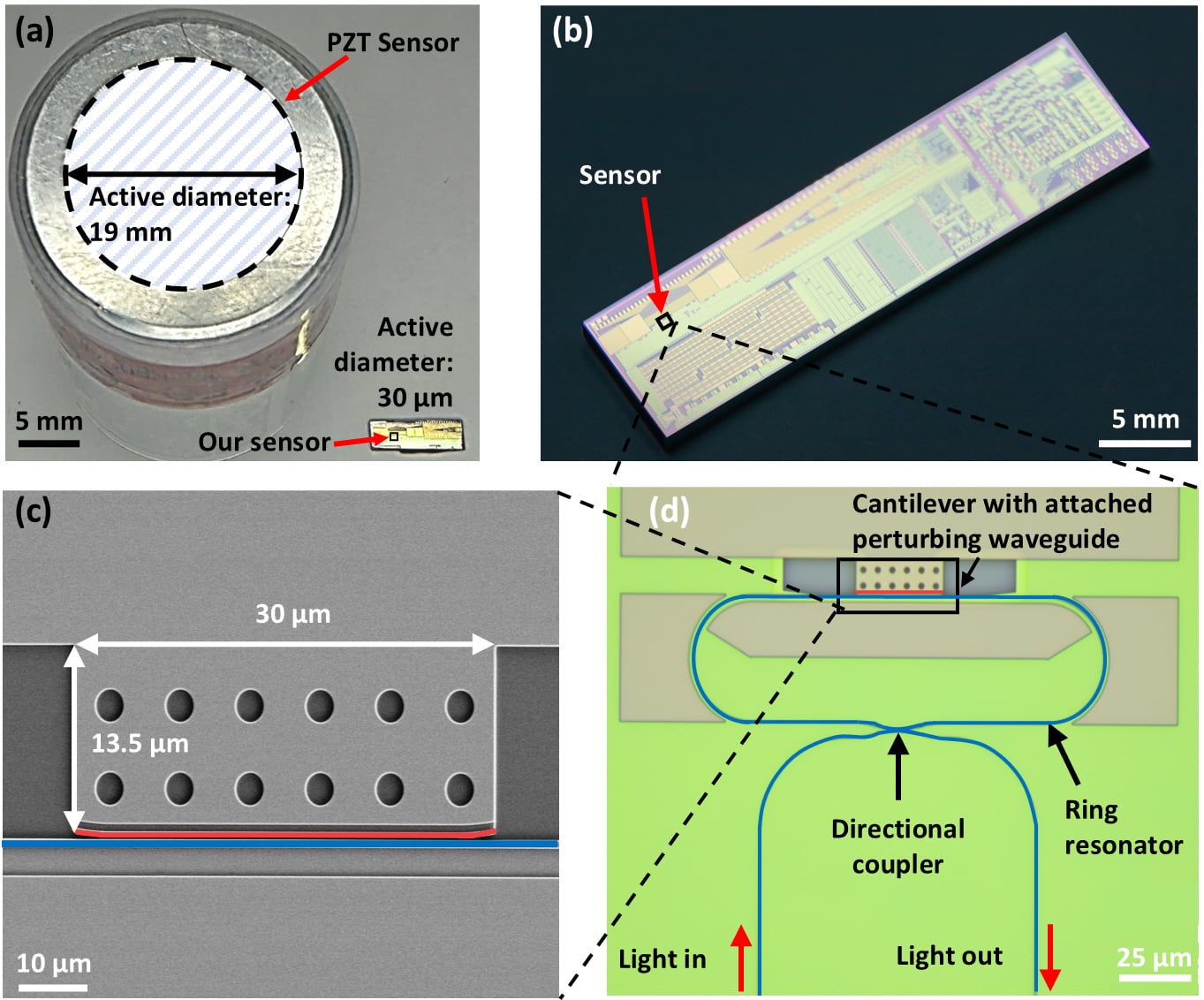
□ A joint research team led by Professors Sangyoon Han and Jaesok Yu of the Department of Robotics and Mechatronics Engineering at DGIST (President Kunwoo Lee) has developed the world’s first miniature optical ultrasonic sensor that is thinner than a human hair using semiconductor fabrication processes. This sensor can precisely detect megahertz (MHz)-range ultrasound transmitted through the air without directly contacting the target object and is expected to revolutionize nondestructive testing technologies for detecting internal defects in semiconductors and secondary batteries.
□ Ultrasonic nondestructive testing, which detects internal defects without disassembling machinery, generally requires a medium such as gel to be applied to the target object (contact testing) to ensure accurate inspection. However, this method is difficult to apply to advanced components that are sensitive to contamination or damage. A “non-contact” approach that transmits and receives ultrasound through the air has been considered an alternative, but it has a critical limitation: ultrasonic signals weaken rapidly in air. In particular, detecting microscopic defects requires high frequencies (in the MHz range), but signal attenuation becomes more severe as the frequency increases. As a result, developing a sensor that combines “high-frequency operation, high sensitivity, and miniaturization” has long been a major challenge.
□ The research team achieved a breakthrough in addressing this problem by using an optical approach that detects minute vibrations caused by sound (ultrasound) using light. Using “silicon photonics,” a technology widely used in the semiconductor industry, the team integrated both an optical circuit through which light travels and a micromechanical structure (an ultrathin cantilever) that vibrates in response to sound onto a single semiconductor chip.
□ When ultrasound reaches the sensor and causes the micromechanical structure to vibrate up and down, the wavelength and intensity of the light passing alongside it change slightly. The sensor detects these changes in light and converts them into an ultrasonic signal. This is the first time in the world that an “optomechanical ultrasonic receiver” has been realized on a single chip using a single semiconductor fabrication process, without the bulky lens components or complex assembly processes required by conventional optical sensors.
□ The developed sensor delivers exceptional performance despite having a sensing area of just 0.0004 mm² (30 μm × 13.5 μm), which is thinner than a human hair. Its receiving responsivity per effective sensing area was measured to be more than 25,000 times higher than existing commercial ultrasonic sensors. Its ultra-high-sensitivity design thus overcomes the physical limitation of signal attenuation in air.
□ A major advantage of this technology is that it can be mass-produced using existing 8-inch silicon wafer semiconductor foundry (contract manufacturing) infrastructure without modification. By simply changing the design layout, sensors operating at different frequencies can be fabricated simultaneously on a single wafer, making this technology a key proprietary technology that could expand the silicon photonics ecosystem beyond its traditional focus on communications to applications in industrial instrumentation and medical imaging.
□ Professor Sangyoon Han of the Department of Robotics and Mechatronics Engineering at DGIST said, “This study demonstrates that an ultrasonic sensor can be created using a single semiconductor device without the need for complex assembly of multiple components. Going forward, we will develop this technology into a high-density array-type optical ultrasonic system that integrates dozens of receivers on a single chip.” Professor Jaesok Yu said, “We plan to expand the applications of this technology beyond non-contact inspection of contamination-sensitive semiconductor wafers, secondary batteries, or composite materials to the fields of medical and bioimaging.”
□ This research was supported by the Samsung Science & Technology Foundation and a program of the National Research Foundation of Korea. DGIST Professors Sangyoon Han and Jaesok Yu and KAIST Professor Jungwon Kim served as corresponding authors, while DGIST integrated master’s and doctoral program student Sangwoo Nam and Dr. Jae Hyun Kim served as co-first authors. The study, conducted in collaboration with Professor Changho Lee’s research team at Chonnam National University, was published in September in Photonics Research, a renowned international journal in the field of optics.