Structure and operational mechanism of the optoelectronic synaptic device based on the designable van der Waals crystal operating with light.
A research team led by Professor Taesung Kim of the School of Mechanical Engineering at Sungkyunkwan University (SKKU, President Ji-beom Yoo) developed an optoelectronic synaptic device that mimics the functions of human neurons and synapses at the device scale. The researchers designed a designable van der Waals (vdW) crystal through a single-step sulfurization process using mixed plasma. The developed device operates under optical stimuli, offering a structural solution to configure semiconductor materials for brain-inspired computing.
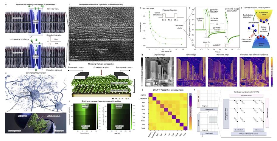
Rapid advancements in artificial intelligence and hyper-connectivity require neuromorphic vision systems capable of sensing and processing vast amounts of visual data in real time. Optoelectronic synapses, which exhibit conductance variations in response to light signals, serve as core components of these systems. Layered vdW materials attracted significant attention as promising candidates due to their excellent optical properties and atomic-scale thickness. However, conventional vdW materials faced technical challenges, including the difficulty of precisely controlling grain boundaries and intercalation, polymer residue accumulation, mechanical warpage at interfaces, and poor large-area crystalline uniformity.
To overcome these limitations, the research team focused on the structural similarity between light-sensitive ion channels in biological membranes and layered vdW lattices. The researchers applied an argon and hydrogen sulfide (Ar + H₂S) plasma sulfurization process to bulk van der Waals rhenium selenide (ReSe₂). This single-step process transformed the upper portion of the material into a nano-crystalline ReSe₂ layer composed of nano-sized grains, while preserving the underlying bulk single-crystalline ReSe₂ layer without damaging the interlayer interfaces. These two integrated layers structurally correspond to the light-sensitive ion channels of a neuronal cell membrane and the intracellular environment, respectively, and were fabricated without additional deposition or patterning steps.
The research team utilized scanning probe microscopy (SPM) to resolve the pathways of S²⁻ (sulfur) ionic migration. The grain boundaries in the nano-crystalline ReSe₂ layer confined the sulfur ionic transport at the atomic scale, enabling deterministic control over synaptic weight updates, similar to the gating mechanism of biological ion channels. The device demonstrated key synaptic functionalities, including multi-level conductance modulation, long-term potentiation/depression (LTP/LTD), paired-pulse facilitation (PPF), and a tunable short-term to long-term memory (STM-LTM) transition. The nano-crystalline ReSe₂ device exhibited a 34.7% increase in retention efficiency during learning-forgetting-relearning cycles compared to bulk ReSe₂. In system-level evaluations, the device successfully performed edge detection on natural images and achieved a 96.24% classification accuracy on the CIFAR-10 image recognition task. This development offers a materials platform for next-generation neuromorphic semiconductors and AI hardware.
"This study demonstrates a single-step method to design the structure of van der Waals crystals for optoelectronic synaptic devices that learn and store information using light," said Professor Taesung Kim, the corresponding author of the study. "By structurally resolving the random nature of ionic migration and interfacial issues inherent in conventional devices, this architecture can be applied to research on next-generation neuromorphic semiconductors and AI hardware."
This research received financial support from the National Research Foundation of Korea (NRF) Leader Research Program, the Institute for Basic Science (IBS), and the Semiconductor-Track Graduate School Program funded by the Ministry of Trade, Industry and Energy (MOTIE). The study was conducted as a collaborative effort among researchers from Sungkyunkwan University (SKKU), the Center for Quantum Nanoscience at IBS, and the Korea Institute of Machinery and Materials (KIMM). The findings were published online in the international journal Advanced Materials (Impact Factor: 26.8, top 1% in JCR) on June 3, 2026.