□ DGIST (President: Kuk Young) announced on Wednesday, November 1, 2023, that Dr Heo Su-jin and Prof. Jang Jae-eun’s research team, affiliated to the Department of Electrical Engineering and Computer Science, developed an ultra-small nano vacuum tube transistor. As the developed transistor can stably operate in atmospheric pressure without being affected by extreme external environments, it is expected to contribute to the groundbreaking development of various fields such — as aerospace, artificial intelligence (AI), 6G wireless communications, and self-driving vehicles.
□ A vacuum tube, known as the first electronic device, is used to switch, amplify, or commutate electric signals. In the past, vacuum tubes functioned as a main part of a diverse range of electronic devices, including ENIAC, the first computer, radios, and televisions. Although vacuum tubes are still used in a few specialty fields requiring high frequency and great electric power, most of them have been replaced with semiconductor transistors based on solid silicone due to problems such as high electricity consumption, intense heat generation, and large size (a low degree of integration).
□ However, silicone-based semiconductor transistors have limitations in operational speed, due to material properties, and are sensitive to external environments, resulting in rapid property changes and permanent damage to concerning related device. These challenges lead to hindrances in the broad application of silicone-based semiconductors, emphasizing the need to develop an advanced electronic device based on new materials and operational principles.
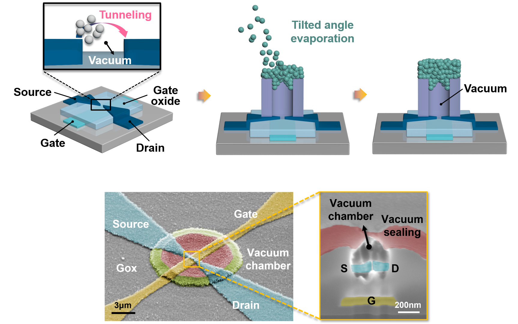
□ Under these circumstances, Prof. Jang’s research team proposed an ultra-small nano vacuum tube transistor that combines the principles of existing vacuum tubes with modern semiconductor production technologies. The proposed transistor uses a vacuum condition as a channel (or the medium of electron transport) and operates based on quantum mechanical tunneling to solve the essential problems of silicone-based semiconductor transistors. Nano processing technology was also utilized to miniaturize a vacuum device to approximately a nanometer in size. Furthermore, the research team invented a vacuum sealing film formation technology to overcome the limitations of existing vacuum transistors which can only operate in a vacuum state. Based on this technology, they developed an ultra-small vacuum tube, miniaturized with a volume of approximately 100 billionths of 1 liter to support the stable operation of the proposed transistor.
□ The developed ultra-small vacuum tube maintained a high vacuum level with a high degree of reliability in atmospheric pressure. Accordingly, the nano vacuum transistor attached to it operated successfully in various extreme conditions without using additional special devices. In particular, the developed transistor exhibited stable operational properties despite changes in extreme external environments, such as a wide range of temperature (from –173°C to 120°C), X-rays, and ultraviolet rays.
□ The nano vacuum tube transistor proposed by Prof. Jang’s research team is highly compatible with existing complementary metal-oxide semiconductor (CMOS) processes and can be easily manufactured, thereby showing its potential to serve as an alternative solution for the problems of existing semiconductor technologies. It is also expected to contribute to developing next-generation electronic devices that can be used in highly advanced electronic equipment during the present era, where electronic devices have become indispensable.
□ Prof. Jang stated that “the ultra-small nano vacuum tube transistor developed in our research is a novel technology that can remove barriers against the practical application of vacuum devices.” He added the “researchers, including those from the National Aeronautics and Space Administration (NASA), have constantly conducted research on developing advanced semiconductor technologies and replacing existing semiconductor technologies. It is anticipated that the developed transistor will serve as a crucial solution in the recently emerging aerospace field and the extensive next-generation electronic device field.”
□ The research paper on the developed transistor was supported by the Industry-University Project Support Program, operated by Samsung Electronics, and published in the online edition of ACS Nano (IF = 18.027), a highly recognized international academic journal in the field.
- corresponding author e-mail address : [email protected]