
This story is featured in the Asia Research News 2021 magazine. Read in ISSUU (above) or full text and images below.
Scientists at The Chinese University of Hong Kong (CUHK) have developed a new printing method that can make fabricating integrated circuits and other tiny devices easier and cheaper. The approach overcomes issues in conventional micro-manufacturing processes, which require multiple steps, advanced equipment and highly trained personnel, and are prone to errors.
“Our new approach directly prints patterns onto substrates,” says Sen Yang, a physicist at CUHK who led the research, which was published in the journal Nature Communications. “We can print metals, insulators, and magnets from the macroscopic scale all the way down to a few nanometres in size. For example, the method can be used to print an electric circuit on a glass slide or even on normal tape, while retaining electrical properties as good as the bulk metal and having the flexibility of materials like nylon.”
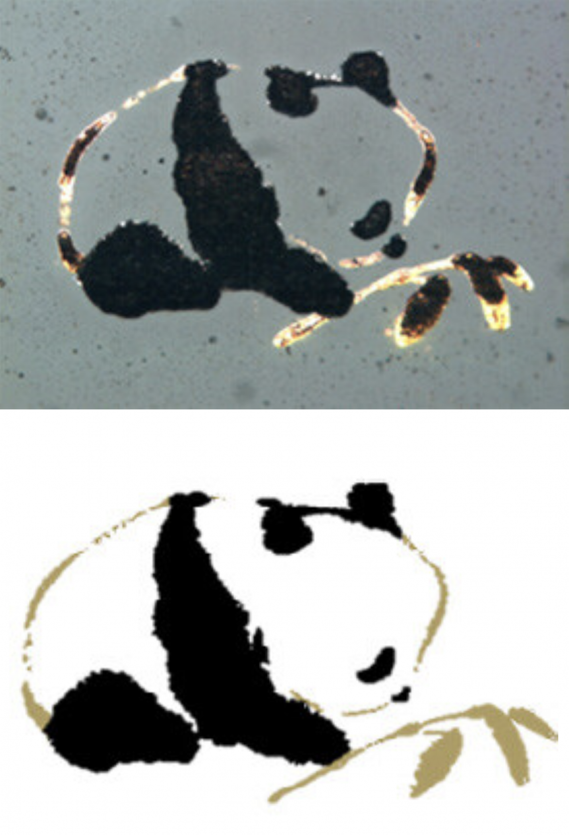
The method involves depositing a mixture of two solutions containing metal particles and semiconductor nanoparticles onto a surface. Laser light shone on the surface induces a reaction that causes the metal particles to stick to the surface of the nanoparticles, and then to attach to the spot focused on by the laser. Once the patterning is done, the liquid part of the solutions is removed and the surface is cleaned, leaving a printed pattern. For example, the panda printed in platinum and gold (top) matches the design (bottom).
The method, called light-induced material deposition, starts with depositing onto a surface a mixture of two solutions, one containing metal particles and the other containing semiconductor nanoparticles. The scientists found their process works on a wide range of surfaces, including glass, quartz, sapphire, indium tin oxide, and tape. The metal particles in the first solution can be gold, platinum, silver, iron, zinc or nickel. Also, a wide range of nanoparticles can be used for the second solution. Interestingly, the researchers found commercial ink, which contains carbon-based nanoparticles, works surprisingly well for this purpose.
Next, laser light is shone on the deposited mixture and moved over it to give the desired pattern. The laser light excites electrons in the nanoparticles, inducing a chemical reaction that cause the metal ions to stick to them. The laser light also acts like an optical tweezer, trapping the metal/nanoparticle compound on the printing surface precisely where the laser is focused. Once the pattern is complete, the extra solution is removed and the surface cleaned, leaving the finished printed structure.
A series of tests confirmed the quality of the deposited materials and their electrical and mechanical properties. The scientists used the method to print a variety of structures, including a resistor flex sensor commonly used in robotics. The approach is cheap, versatile, and easy to use, so much so that it would be possible to print electrical circuits in the field. It could also make repairing electrical circuits easier than current approaches.
The scientists are now trying to improve the process so it can print even smaller structures, down to 20 nanometres in size. “We will also try to further simplify the setup and make a market-ready prototype, with the aim of commercializing our product within five years,” says Yang.
Further information
Assistant Professor Sen Yang
[email protected]
Department of Physics
The Chinese University of Hong Kong