□ The Institute of Next-Generation Semiconductor Convergence Technology (Director Kim Dae-hwan) at DGIST (President Lee Kunwoo) has been selected for the “Project for Utilizing Highly Experienced Professionals to Support Semiconductor Technology Development,” a new project under the “2026 Nano and Materials Technology Development Program: Infrastructure Development (Fab Advancement),” organized by the Ministry of Science and ICT and National Research Foundation of Korea.
□ This project is implemented to apply the expertise of highly experienced professionals, having over 10 years of know-how in semiconductor industrial sites, to public fab operations and technology development. As the lead research and development (R&D) institution, DGIST plans to employ their expertise to lead efforts to strengthen public fab-based technical support for industry-academia-research institute collaborations, including (1) developing semiconductor process technologies and streamlining fab operations; (2) stabilizing the operation of equipment and fab facilities; (3) providing support for devices, design, analysis, feature assessment, and multi-project wafer (MPW) fabrication; and (4) providing consulting and on-site technical support related to semiconductor technology development.
□ Through this, DGIST plans to establish a public-fab-based life-cycle technical support system, transcending the existing public fab’s support system focused on unit processes, so that researchers and companies can conduct reliable semiconductor R&D and validation. The project has a total budget of 7.2 billion won over six years, and DGIST, as the lead R&D institution, has secured 4.2 billion won in research funding. Seoul National University is participating as a co-R&D institution.
□ “This project is highly significant in that it directly links the know-how of highly experienced professionals, who have accumulated extensive experience in industrial sites, to public fab technology development and operation enhancement,” stated Kim Dae-hwan, Director of the DGIST Institute of Next-Generation Semiconductor Convergence Technology. “Building on our capabilities in the 6-inch silicon (Si) CMOS-based MPW and research foundry we have built, DGIST will strengthen process-related collaboration with Seoul National University and contribute to vitalizing the national semiconductor research ecosystem.”
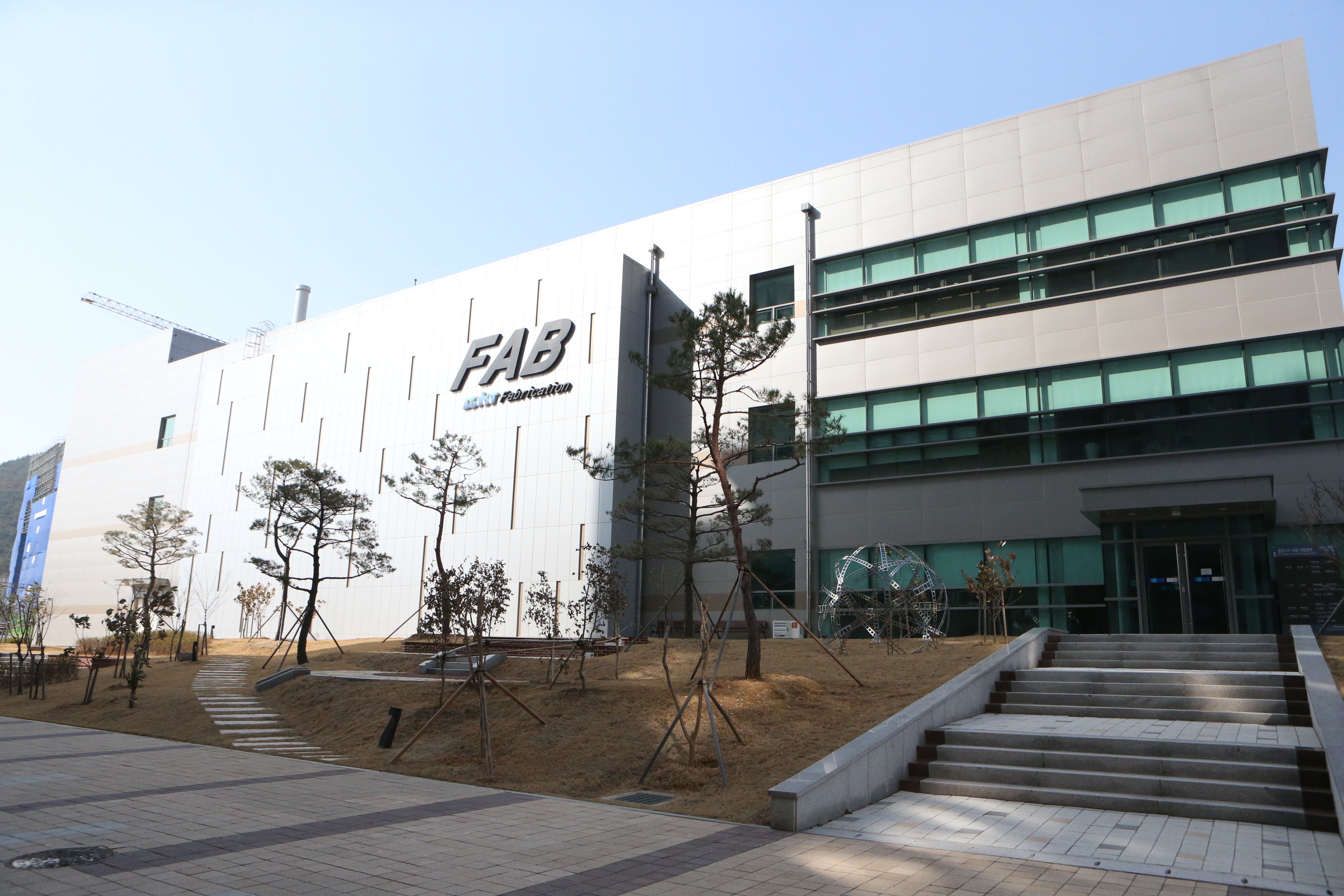
□ The DGIST Institute of Next-Generation Semiconductor Convergence Technology is a national nano-infrastructure hub institution, which has a batch processing infrastructure capable of 6-inch wafer-based Si semiconductor front-end processes, as well as capabilities in integrating semiconductor design, processing, and analysis. Through projects such as a semiconductor design and verification infrastructure activation project, MPW fabrication support, and a service for shared use of public fab, the institute has been providing research support services—spanning from semiconductor design to fabrication, measurement, and analysis—to researchers for industry-academia-research institute collaborations.
□ Lee Sang-han, Team Leader of the DGIST Nano-fab Support Team and principal investigator for this project, stated, “Through this project, we plan to combine the on-site experience of highly experienced professionals with DGIST’s public fab infrastructure to more actively support semiconductor R&D, stabilize fab operations, provide technical support for industry-academia-research institute collaborations, and cultivate semiconductor professionals.”