
DGIST Professor Dongwon Yun at the Department of Robotics Engineering
A research team led by DGIST Professor Dongwon Yun at the Department of Robotics Engineering has developed a new process technology that can freely imprint fine circuit patterns on polymer substrate, a necessary component of electronic products. This study was jointly conducted by an international team of researchers, including Professor Woosoo Kim’s team at Simon Fraser University in Canada, and PROTEM. Hot embossing process technology, which is used to imprint fine circuit patterns of nm and μm size on flexible polymer substrate, is a technology applied for mass imprinting of precise patterns at a low unit cost. However, it can imprint circuit patterns that are imprinted beforehand on the pattern stamp, and the entire expensive stamp must be changed to put different patterns. In this study, the team succeeded in developing a new process method that overcame the weaknesses of the conventional process. First, the team used electromagnetic theory and developed an electromagnetic actuator that can apply tens of MPa pressure needed for the hot embossing process on the film. After, the team fixed the actuator at the desired location on the film heated by heating device such as hot plate and successfully developed a precise location control system that can imprint patterns, completing a new process technology. With this new technology, tens and hundreds of μm-sized fine circuit patterns can be imprinted on the desired location in a desired shape, which can help reduce the additional cost and time caused by pattern change. It is also expected to enhance equipment compatibility as it can be used with the existing process equipment as well as to be used widely in related process fields. Professor Yun said “The process technology we have developed can freely imprint desired fine circuit patterns on flexible polymer electronic substrate without any additional replacement, so it is more economic and efficient than the existing process for imprinting patterns. We will continue do to a follow-up research on this process technology so that it can be used in various areas of electronic and display industry such as semiconductor, flexible electronic display as well as manufacturing process.” He also added that “This new impact print-type hot embossing process technology will be able to form diversified fine circuit patterns more easily, so it is expected to contribute to the technology development of bio and medical R&D field since it can create more various patters in real-time.” This study been published on the internal cover of ‘Advanced Engineering Materials’, an international journal of materials and engineering, on September 24. The research was carried out with the support by the Ministry of Trade, Industry, and Energy as an international joint R&D project. For more information, contact: Dongwon Yun, Assistant Professor Department of Robotics Engineering Daegu Gyeongbuk Institute of Science and Technology (DGIST) E-mail: [email protected]
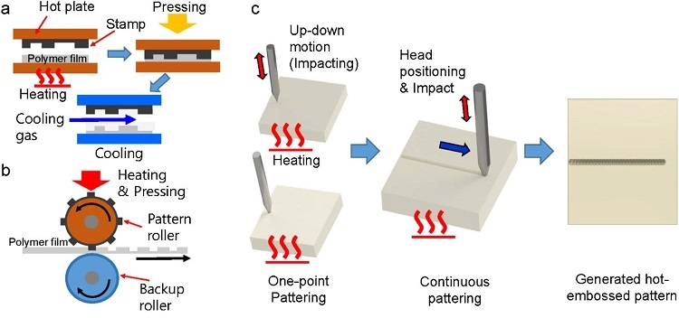
Conceptual diagram for the hot embossing process. a) Plate-type hot embossing. b) Roll-to-roll hot embossing. c) Proposed impact-type hot embossing
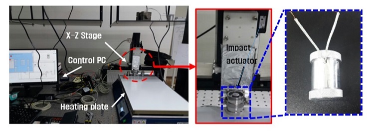
Experimental apparatus for impact-type hot embossing experiment