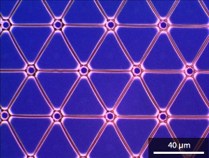
Optical microscopy image of a fully connected hexagonal network of microwires prepared by the self-assembly of gold nanoparticles on a photoresist template.
Materials that conduct electricity but which are also transparent to light are important for electronic displays, cameras and solar cells. The industry’s standard material for these applications is indium tin oxide (ITO), but the spiraling cost and limited supply of indium has prompted a search for alternatives.
One promising approach is to build mesh-like networks of ultrathin conducting metal wires that light can pass through. Ivan Vakarelski at the A*STAR Institute of Chemical and Engineering Sciences and Xiaosong Tang and Sean O’Shea at the A*STAR Institute of Materials Research and Engineering[1] have now refined the process of making these tiny meshes so that it is feasible for large-scale manufacturing.
The secret to fabricating such intricate microstructures is to encourage metal nanoparticles to assemble themselves from a liquid suspension. This requires a predefined template to guide the self-assembly—in the same way that coffee granules assemble into a ring under a cup as spilt liquid evaporates.
A few years ago, Vakarelski and his co-workers demonstrated the possibility of using latex microparticles as a template for such a mesh using a solution containing gold nanoparticles. “As the solvent evaporated, a liquid bridge network developed around the latex particles, leaving behind a network of microwires formed by the self-assembly of the gold particles,” explains O’Shea. “This is an easy approach for research purposes, but is difficult to control on a manufacturing scale.”
To tackle this problem, the researchers turned to the technique of photolithography, which involves using ultraviolet light to draw patterns in a photoresist film. The exposed and hardened parts of the photoresist then act as a precise template for self-assembly of gold nanoparticles. “It is difficult, however,” says Vakarelski, “to produce spheres replicating the latex particle template using photolithography. We tried several alternative structures and found that arched structures work just as well.”
Using photolithography to produce a template of arch-like structures and the same solution of gold nanoparticles, the researchers prepared a high-quality gold microwire mesh (pictured) with conductance and transparency comparable to those of high-grade ITO. “An added advantage of the arched structures is that, unlike latex microparticles, we are not restricted to a hexagonal network topology,” says O’Shea. Indeed, the researchers successfully produced networks of rectangles, hexagons and triangles. “Using this technique we plan to explore special functional networks using other types of particles, including semiconducting particles, magnetic particles, carbon nanotubes, DNA and proteins,” says Vakarelski.
The A*STAR-affiliated researchers contributing to this research are from the Institute of Chemical and Engineering Sciences and Institute of Materials Research and Engineering