A study of oxygen molecules interacting with atomically thin layers of materials being developed as new generations of semiconductors could significantly improve control over the fabrication and applications of these ‘two-dimensional’ (2D) materials. The work, by researchers at Daegu Gyeongbuk Institute of Science and Technology (DGIST), in South Korea, with colleagues elsewhere in South Korea and in Japan, is published in the journal Advanced Science.
The single layer of bonded atoms that comprise 2D materials can have semiconducting properties suitable for making electronic components including transistors on much smaller scales than generally possible. This could move microelectronics down into the nanoelectronics level, building tiny and more efficient circuits, including flexible devices and solar cells.
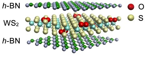
Some of the most promising 2D materials are ‘transition metal dichalcogenides’ (TMDs), which have elements from the transition metal groups of the periodic table combined with twice as many ‘chalcogen’ elements, especially sulfur, selenium and tellurium. The DGIST team and their colleagues worked with monolayer TMD crystals of tungsten and sulfur, with the formula WS2.
They investigated the tendency of oxygen molecules to become adsorbed onto the defect sites of crystals – sulfur vacancies where a sulfur atom is missing from WS2 lattice sites. They explored the interactions between the defects and oxygen molecules with a technique called electron energy loss spectroscopy (EELS). This uses an electron microscope to fire electrons through the material, then analyses the patterns of energy loss by the electrons to reveal crucial structural information. The EELS results were combined with insights from optical analysis and theoretical calculations.
The researchers paid particular attention to the ability of adsorbed oxygen molecules to become fixed in place when the WS2 crystals were encapsulated within monolayers of another material - hexagonal boron nitride (h-BN) – above and below the WS2 layer. h-BN is a common ingredient of electronic and photonic devices constructed using 2D TMDs.
Fixing the oxygen molecules in place at the defect sites alters and stabilizes the electronic behaviour of the TMDs in a process called passivation. This affects the crystals in subtle ways that will influence their activity in a range of applications.
“Our work provides a new insight into the defect-related phenomena in 2D TMDs, that can trigger revolutionary approaches to control the defect states,” says semiconductor and nanophotonics specialist Prof. Chang-Hee Cho of the DGIST team.
“We now hope to develop new experimental approaches and techniques to control the defect states of the 2D TMDs using h-BN encapsulation,” adds Cho. “This will allow us to move the method towards being ready for full-scale development and eventual commercial uses.”
- Ccorresponding Author E-mail Address : [email protected]
More information: Jin-Woo Jung et al., Defect Passivation of 2D Semiconductors by Fixating Chemisorbed Oxygen Molecules via h-BN Encapsulations, Advanced Science (2024). DOI: 10.1002/advs.202310197
Advertisement