□ DGIST (President Yang Kook) Professor Hongki Kang of the Department of Electrical Engineering & Computer Science and his research team successfully developed a selective photothermal layer formation technology and a transparent electrode based on the fine inkjet printing solution process. This technology is anticipated to contribute to the development of biomaterial devices for applications that require device transparency or are sensitive to temperature changes.
□ Recently, there has been significant interest in a ‘‘transparent electrode’ that facilitates bio-imaging and is applicable in various sectors, such as optogenetics. However, ink material used in existing transparent electrodes, such as indium tin oxide (ITO) or antimony tin oxide (ATO), require processing temperatures of 350 ℃ or above, which is higher than the transition temperature (150–200 ℃) of flexible boards. Therefore, using existing ink material to proceed with transparent electrode processing results in a mechanical weak point of the hardening of the flexible board due to the high temperature.
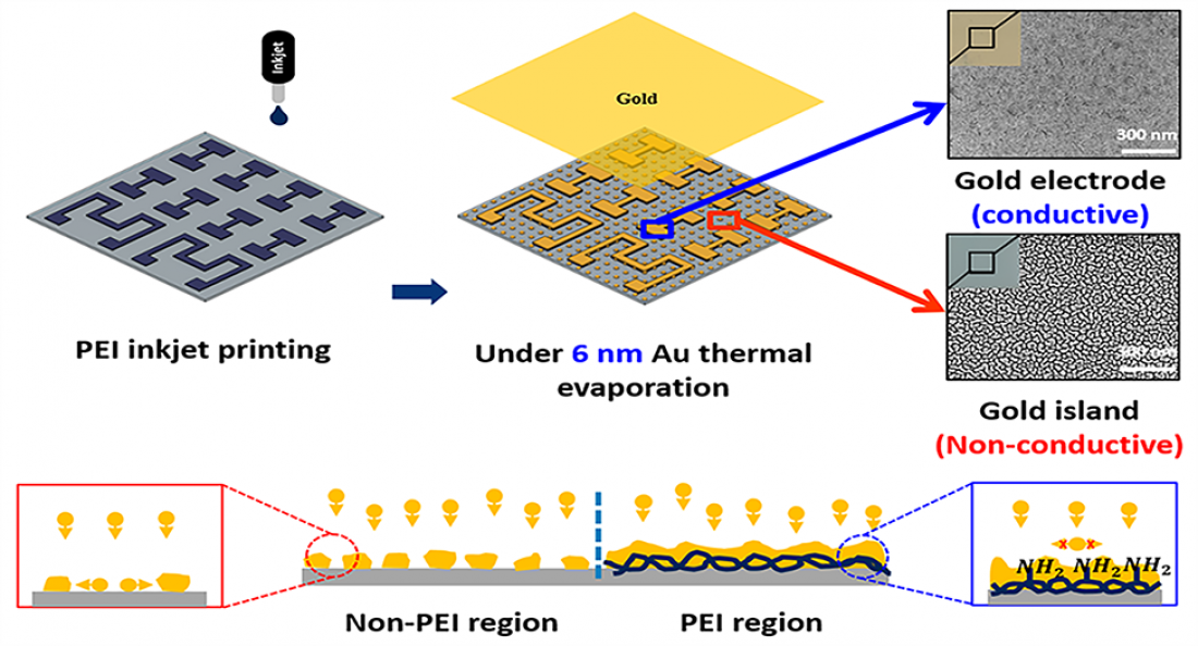
□ Thus, the research team used inkjet printing technology with a high degree of freedom in pattern formation to propose a new method of fabricating a transparent ultra-thin-film gold fine electrode customized for patients. Unlike the existing method of directly printing ink, this technology involves inkjet printing of a polymeric seed layer to induce ganglia generation, and ‘ultra-thin-film gold’ of 6 nm or below is evaporated without a photomask to selectively process a transparent electrode with high penetrance. Simultaneously, a ‘non-conducting gold island layer’ is formed in the area where the polymeric seed layer is not printed, which can be implemented for photothermy. The research team proceeded with verification to identify the completeness of the developed nanostructure. Photothermy was detected using a transparent temperature sensor, and nerve cells were grown on the upper part of the device to identify both bio-suitability and potential for bio-imaging.
□ The ‘ultra-thin-film gold electrode and gold nanostructure’ developed in this study is advantageous compared to existing devices because processing is available at room temperature without using an exposure mask in the fields of engineering application and biomedicine where ‘patient-customized flexible and wearable transparent electrode formation’ is required. The research team anticipates that an expansion of these technologies could lead to successful thermotherapy based on photothermy, such as optics-based PCR, neuromodulation, cancer treatment, and drug delivery.
□ DGIST Professor Hongki Kang of the Department of Electrical Engineering & Computer Science stated that “the key is that this patient-customized ‘ultra-thin-film gold electrode’ can be produced using inkjet printing, which is different from the existing electrode formation method,” and revealed that “it is anticipated that various body signals could be more efficiently measured using this technology through a patient-customized flexible fine electrode array.”
□ This research was supported by the Basic Research Laboratory project supported by the Ministry of Science and ICT through the National Research Foundation of Korea, the 2023 Institute of Science and Technology joint research project, and as an original institutional project of the DGIST. For this research paper, Doohee Kim, who was enrolled in the integrated Master’s and PhD program in the Department of Electrical Engineering & Computer Science at the DGIST, participated as the main author, and the paper was published online in the renowned international journal Electrical Engineering & Computer Science.
Correspondence Author Email Address : [email protected]
1) Non-conducting gold island layer: An island layer formed when gold is evaporated on an area where a polymeric seed layer is not printed, and it is suitable for use as the photothermy layer because it is in island form.


