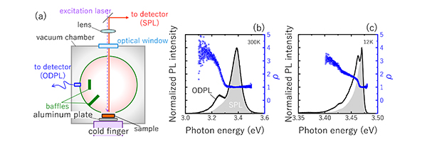
(a) A scheme of temperature variable ODPL spectroscopy. The spectra of ODPL and SPL as well as r (ODPL intensity divided by SPL intensity) measured at (b) T =300 K and (c) T = 12 K.
"Our findings confirm the accuracy of ODPL measurements and show the possibility to measure optical absorption of crystals by the ODPL method, making the process much easier," says Tohoku University materials scientist Kazunobu Kojima.
Huge strides have been made in the development of highly efficient electronic and optical devices, e.g. ultraviolet, blue, and white light-emitting diodes (LEDs) as well as high-frequency transistors, that use nitride semiconductors--specifically aluminum gallium nitride (AlGaN), indium gallium nitride (InGaN), and gallium nitride (GaN).
GaN is a suitable material for power devices on account of its large bandgap energy, high breakdown field and high saturation electron velocity.
There is a strong need for manufacturers to be able to detect crystal defects and test their efficiency. Within such high quality crystals, the concentration of nonradiative recombination centers (NRC) serves as a good predictor of the crystals quality.
Annihilation spectroscopy, deep-level transient spectroscopy and photoluminescence (PL) spectroscopy are among the estimation techniques for detecting point defects which are the source of NRCs. PL spectroscopy is attractive because it requires no electrodes and contacts.
First proposed by Kojima and his research team in 2016, ODPL is a novel form of PL spectroscopy that measures PL intensity by using an integrating sphere to quantify the quantum efficiency of radiation in sample semiconductor crystals. It is non-touching, non-destructive and good for large-sized GaN wafers for room-lighting LEDs and transistors for electric vehicles. Yet, the origin of the two-peak structure formed in ODPL had remained elusive until now.
Kojima and his team combined ODPL and standard PL (SPL) spectroscopy experiments on a GaN crystal at various temperatures (T) between 12 K and 300 K. The intensity ratio (r) of the ODPL spectra to SPL spectra for the NBE emission of GaN showed a linearly decreasing slope for photon energy (E) below a fundamental absorption edge energy (Eabs).The slope obtained in r corresponded to the so-called Urbach-Martienssen (U-M) absorption tail, which is observed in many semiconductor crystals.
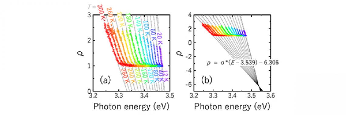
(a) The intensity ratio spectra for various temperatures, where a part of the spectrum of intensity ratio with the steepest slope extracted for each temperature. (b) The intensity ratio spectra for various temperatures with the extrapolations of the extracted slopes, which were converged at a common point: (3.539 eV, -6.306).
Therefore, the origin of the two-peak structure in the ODPL spectra around the NBE emission of the GaN crystal exists because of the U-M tail.
Contact:
Kazunobu Kojima
Institute of Multidisciplinary Research for Advanced Materials
Tohoku University
Email: [email protected]
Advertisement