From left are Distinguished Professor Feng Ding and Leining Zhang from the Center for Multidimensional Carbon Material (CMCM), within the Institute for Basic Science (IBS, South Korea) at UNIST.
What makes something a crystal? A transparent and glittery gemstone? Not necessarily in the microscopic world. When all of its atoms are arranged in accordance with specific mathematical rules, we call the material a single crystal. Like the natural world has its unique symmetry just as snowflakes or honeycombs, the atomic world of crystals is designed by its own structure and symmetry. This material structure has a profound effect on its physical properties as well. Specifically, single crystals play an important role in inducing material’s intrinsic properties to its full extent. Faced with the coming end of the miniaturization process that the silicon-based integrated circuit has allowed up to this point, huge efforts have been dedicated to find a single crystalline replacement for silicon.
In search for the transistor of the future, two-dimensional (2D) materials, especially graphene have been the subject of intense research around the world. Being thin and flexible as a result of being only a single layer of atoms, this 2D version of carbon even features unprecedented electricity and heat conductivity. However, the last decade’s efforts for graphene transistors have been held up by physical restraints graphene allows no control over electricity flow due to the lack of band gap. Then, what about other 2D materials? A number of interesting 2D materials have been reported to have similar or even superior properties. Still, the lack of understanding in creating ideal experimental conditions for large-area 2D materials has limited their maximum size to just a few mm2.
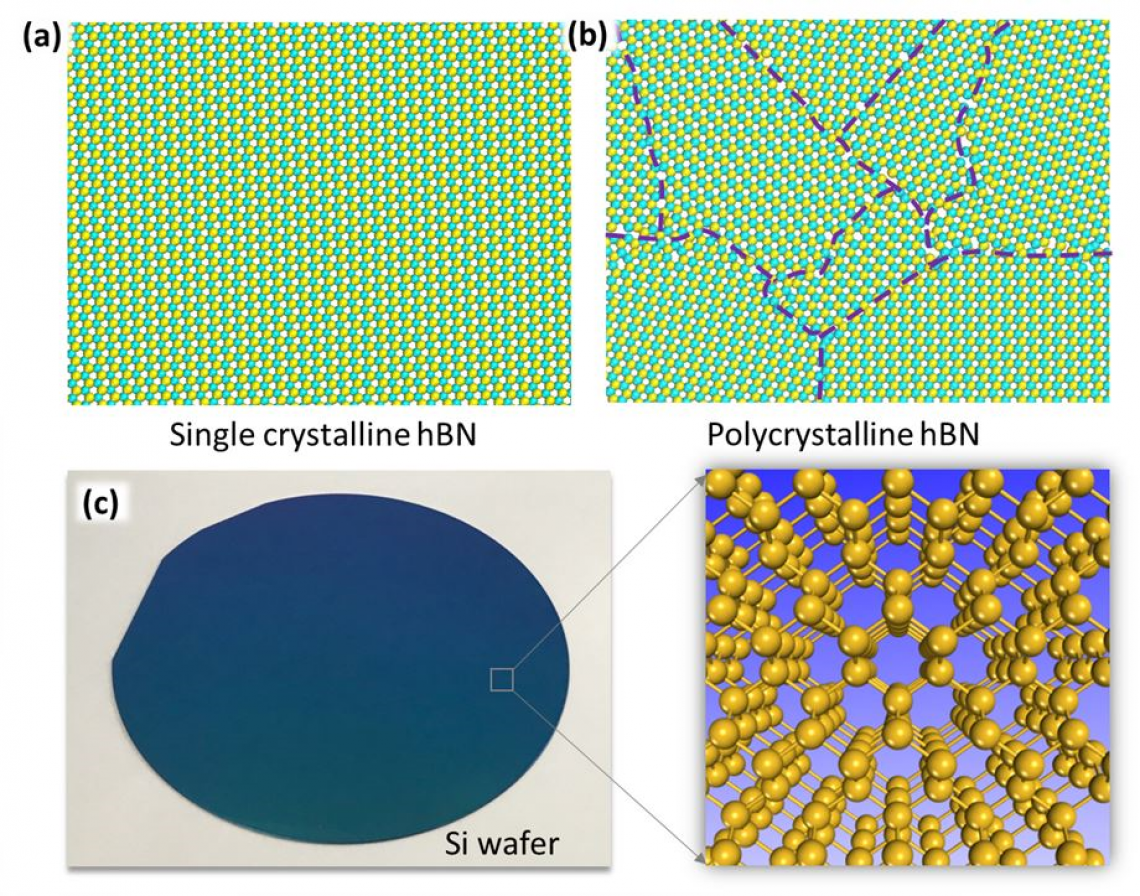
▲ Figure 1. To make a single crystal of 1 mm3 in size, 1021 atoms should be placed precisely in a matrix. (a) Single-crystal hexagonal boron nitride (hBN); (b) polycrystalline hBN; (c) Silicon wafer used in semiconducting industry is a single crystal, in which all the Si atoms form a perfect matrix.
This study has been conducted by Distinguished Professor Feng Ding (School of Materials Science and Engineering, UNIST) and his research team at the Center for Multidimensional Carbon Material (CMCM), within the Institute for Basic Science (IBS, South Korea). Herein, the team announced that they have discovered a novel approach to synthesize large-scale of silicon wafer size, single crystalline 2D materials.
In the study, Professor Ding and Ms. Leining Zhang in collaboration with Peking University, China and other institutions have found a substrate with a lower order of symmetry than that of a 2D material that facilitates the synthesis of single crystalline 2D materials in a large area.
“It was critical to find the right balance of rotational symmetries between a substrate and a 2D material,” says Distinguished Professor Feng Ding, one of corresponding authors of this study. Herein, the researchers demonstrated the successful synthesis of hBN single crystals of 10*10 cm2 by using a new substrate: a surface nearby Cu (110) that has a lower symmetry of (1) than hBN with (3).
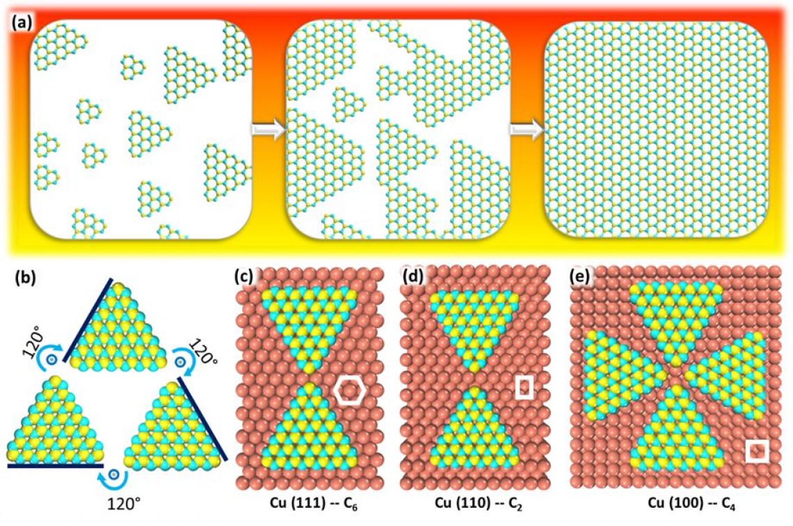
▲ Figure 2. Epitaxial growth of single crystal hBN on a substrate. The hBN islands in (a) are unidirectional. In (b) the 3-fold symmetrical hBN shows 3 times of coincidences during the rotation form 0-360°. hBN has a 3-fold symmetry because the lattice of hBN will not be changed by rotating it by 360°/3 = 120°. (c-e) The equivalent alignments of hBN on copper surfaces (c-e), namely Cu(111), Cu(110) and Cu(100). The top layer atoms of (c),(d) and (e) show equivalent hBN alignments on substrates with 6-, 2-, 4-fold symmetries, respectively. The white shapes show the geometrical characteristic of the substrates, from which the symmetries of the substrates can be seen.
Then, why does symmetry matters? Symmetry, in particular rotational symmetry, describes how many times a certain shape fits on to itself during a full rotation of 360 degrees. The most efficient method to synthesize large-area and single crystals of 2D materials is to arrange layers over layers of small single crystals and grow them upon a substrate. In this epitaxial growth, it is quite challenging to ensure all of the single crystals are aligned in a single direction. Orientation of the crystals is often affected by the underlying substrate. By theoretical analysis, the IBS scientists found that an hBN island (or a group of hBN atoms forming a single triangle shape) has two equivalent alignments on the Cu(111) surface that has a very high symmetry of (6).
“It was a common view that a substrate with high symmetry may lead to the growth of materials with a high symmetry. It seemed to make sense intuitively, but this study found it is incorrect,” says Ms. Leining Zhang, the first author of the study.
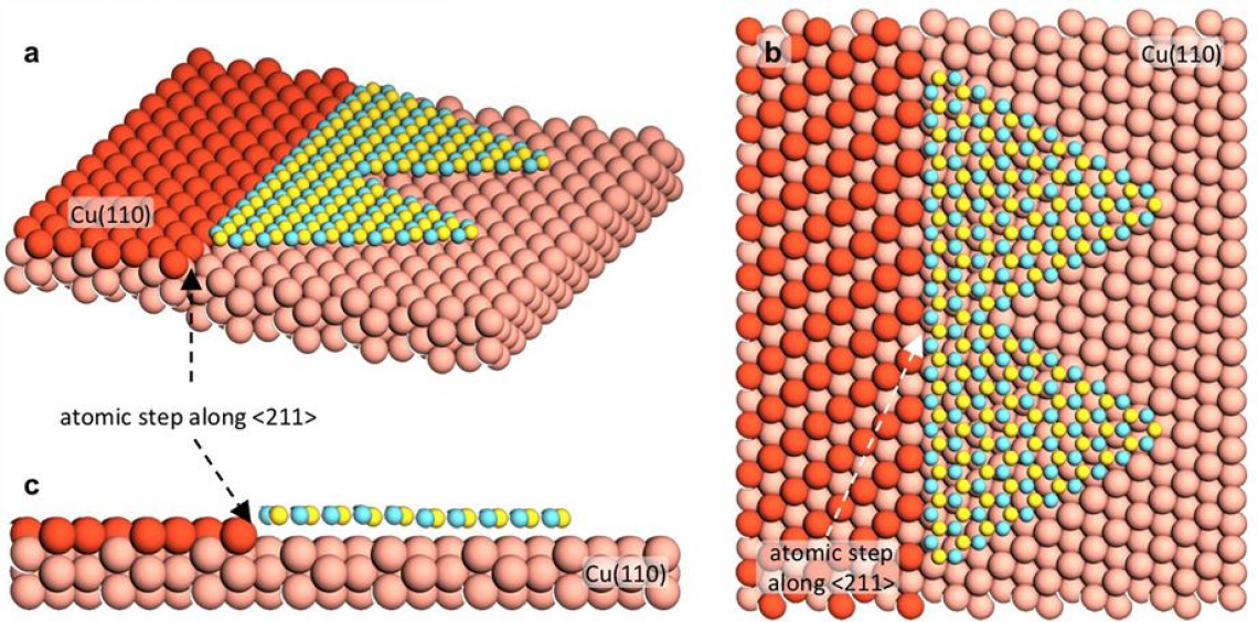
▲Figure 3. Edge-coupling-guided hBN growth on Cu (110). (a–c), schematic of edge-coupling-guided hBN growth on a Cu (110) vicinal surface with atomic step edges along the <211> direction. (b) shows the top view and (c) shows a side view.
Previously, various substrates such as Cu(111) have been used to synthesize single crystalline hBN in a large area, but none of them were successful. Every effort ended with hBN islands aligning along in several different directions on the surfaces. Convinced by the fact that the key to achieve unidirectional alignment is to reduce the symmetry of the substrate, the researchers made tremendous efforts to obtain vicinal surfaces of a Cu(110) orientation; a surface obtained by cutting a Cu(110) with a small tilt angle. It is like forming physical steps on Cu. As a hBN island tends to place in parallel to the edge of each step, it gets only one preferred alignment. The small tilt angle lowers the symmetry of the surface as well.
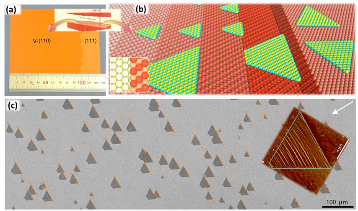
▲ Figure 4. (a) large area single-crystal copper foil with a low symmetric surface, a vicinal surface of Cu(110) orientation, namely V-(110). (b) the growth of large number of unidirectional aligned hBN islands on the vicinal Cu(110) surface. (c) SEM and AFM images of hBN islands on vicinal Cu (110).
The team eventually found that a class of vicinal surfaces of Cu (110) can be used to support the growth of hBN with perfect alignment. On a carefully selected substrate with the lowest symmetry or the surface will repeat itself only after a 360degree rotation, hBN has only one preferred direction of alignment. The research team of Professor Kaihui Liu from Peking University, has developed a unique method to anneal a large Cu foil, up to 10*10 cm2, into a single crystal with the vicinal Cu (110) surface and, with it, they have achieved the synthesis of hBN single crystals of same size.
Besides flexibility and ultrathin thickness, emerging 2D materials can present extraordinary properties when they get enlarged as single crystals. “This study provides a general guideline for the experimental synthesis of various 2D materials. Besides the hBN, many other 2D materials could be synthesized with the large area single crystalline substrates with low symmetry,” says Professor Ding. Notably, hBN is the most representative 2D insulator, which is different from the conductive 2D materials, such as graphene, and 2D semiconductors, such as molybdenum disulfide (MoS2). The vertical stacking of various types of 2D materials, such as hBN, graphene and MoS2, would lead to a large number of new materials with exceptional properties and can be used for numerous applications, such as high-performance electronics, sensors, or wearable electronics.”
Feng Ding
Distinguished Professor, School of Materials Science and Eng., UNIST
IBS Center for Multidimensional Carbon Materials (CMCM)
Dahee Carol Kim
Public Information Officer
T: +82-42-878-8133
E:[email protected]
Story Source
Materials provided by Institute of Basic Science.
Notes for Editors
The online version of the original article can be found HERE.