Featured in Asia Research News 2020 Magazine
Computer-generated holographic images can be better seen from the side thanks to a thin metal film with millions of tiny pinholes. This ‘photon sieve’ could one day enable dynamic 3D images to be viewed on mobile devices.
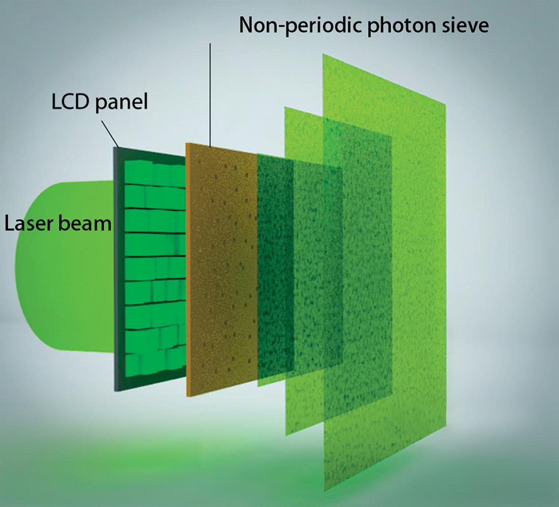
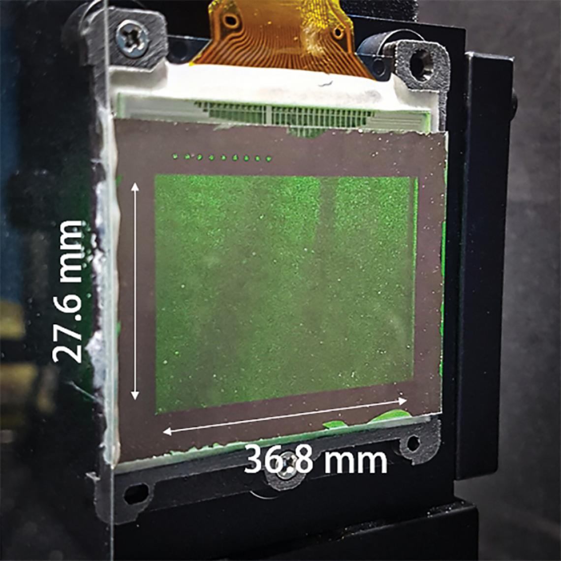
Researchers at the Korea Advanced Institute of Science and Technology (KAIST) in collaboration with SAIT Samsung Electronics placed an array of sub-micron apertures over a commercial LCD panel illuminated from behind with a laser. Light is diffracted widely as it exits the pinholes, allowing holograms to be clearly seen within a viewing angle of 30 degrees.
Users looking at the same scene with the photon sieve removed would experience holograms with a viewing angle of just a few degrees.
“The present demonstration is the first flat-panel holographic display capable of displaying a large-sized image with a wide viewing angle,” says YongKeun Park, who has expertise in holographic microscopy and leads the Biomedical Optics Laboratory at KAIST.
SKINNY 3D
Visually captivating, holograms have immediate appeal as an entertainment medium, but their potential does not stop there.
“3D images contain a wealth of informa- tion, making holograms useful for observing changes in systems,” explains Park. “Displays made using holographic recording techniques could be used for remote surgery, head-up displays for cars, augmented and virtual reality, and more.”
Holographic displays could provide a comfortable, headset-free solution for users in home and work environments. Park anticipates viewers gathering round a flat-panel holographic display, much like people watch a TV or computer screen today.
The rapid advancement of LCDs replacing clunky tube-based TV and computer monitors motivated Park to develop a practical, attractive design for a flat-panel holographic display.
“Making a thin device has become one of the most essential criteria for the display industry,” he notes.
Researchers placed an array of sub-micron aper- tures over a commercial LCD panel illuminated from behind with a laser. Light is diffracted as it exits the photon sieve pinholes, allowing holograms to be clearly seen within a viewing angle of 30 degrees.
PINHOLE POWERED
A key feature of the 3D photon sieve is that each pinhole is positioned to correspond to a pixel in the LCD panel. This means the optical field scattered from each pinhole can be independently modulated pixel-by-pixel, providing finer con- trol of the hologram image.
The pinholes were made using focused ion beams for this study, but can also be manufactured using more cost-effective methods in the future. Each aperture in the array is pseudo-randomly oriented to reduce the likelihood of image distortion and duplication. The precise patterning of the pinhole array makes the device’s calibration and operation more straight-forward.
FIRST IMAGES
The scientists programmed their device to generate holograms of a single-colour tetrahedron and of a rotating cube featuring red, green and blue elements.
The images were produced using a 1024 x 768 pixel display without colour filters. Colours were applied via so-called space division multiplexing: randomly and evenly assigning pixels on the LCD panel to manage light from red, green or blue laser beams aimed at the apparatus.
One of the design’s main challenges is screen brightness. As much as 95% of the light shown through the display is blocked by the photon sieve. In their proof-of-concept experiments, reported in Nature Communications, the scientists used a high-power laser to boost image visibility, but they are also considering other approaches, such as incorporating micro-lenses into their design.
“These could help focus the incident light into the pinholes and enhance transmittance,” explains Park.
Borrowing techniques used to pattern microchips, the photon sieve, which is just 300 nanometres thick and is supported by a glass substrate, is relatively easy to manufacture and scalable. Also, the design features a commercial LCD panel, which adds to its practical appeal.
“Our technique can be easily integrated into the current LCD production process and is a promising approach towards thin holographic displays,” says Park.
The researchers will continue to refine the technology, building on the platform’s industrial promise.
For further information, contact:
Professor YongKeun Park
Biomedical Optics Laboratory
Korea Advanced Institute of Science and Technology
E-mail: [email protected]
Read this story in the Asia Research News 2020 magazine.
The many ways we can tell your research story. Find out more from our Content services page.


