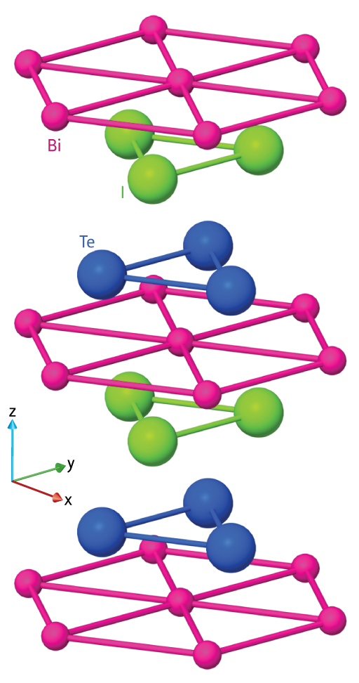
Figure 1: The layered atomic structure of BiTeI creates a three-dimensional version of the Rashba effect, normally seen at only two-dimensional surfaces and interfaces (pink, bismuth; blue, tellurium; iodine, green).
In the developing field of spintronics, physicists are designing devices to transmit data using the inherent axial rotation, or spin, of electrons rather than their charge as is used in electronics. Weak coupling of electron spin to electrical currents, however, makes gaining this level of control difficult. Yoshinori Tokura from the RIKEN Advanced Science Institute, Wako, working with colleagues from across Japan, has now shown that the semiconducting material BiTeI could provide the control needed because of its unusual atomic arrangement1.
Spin can take one of two values, conventionally labeled ‘up’ and ‘down’. Usually, an electron in a state with an up-spin has the same energy as an electron in the equivalent down-spin state. This so-called ‘energy degeneracy’ makes it difficult to control up and down spins independently. “A principle technique in spintronics is to manipulate spin by means of an electric current or voltage,” says University of Tokyo scientist and co-author of the paper Kyoko Ishizaka. “Lifting this degeneracy will enable a number of novel spin-to-current conversion techniques.”
One way to split the energy of the two spin states is to destroy the symmetry of the atomic lattice; at a surface or at the interface between two materials for example. This is known as the Rashba effect. Physicists have observed this effect; however, splitting energy in these two-dimensional (2D) systems was, in general, too small for real applications. Tokura, Ishizaka and their team demonstrated experimentally a Rashba-type effect in three-dimensional, or ‘bulk’, BiTeI. “In 2D Rashba systems, spintronic function is hindered by the electrons away from the surface, which remain degenerate,” explains Ishizaka. “In BiTeI, on the other hand, all the carrier electrons are spin-split.”
The researchers studied BiTeI using a technique called angle-resolved photoemission spectroscopy, whereby electrons excited from the surface of a sample by incoming light provided details about the material’s energy structure. The measurements showed that the spin splitting was large enough to make BiTeI a potential material for various spin-dependent electronic functions. The researchers took a first-principles approach to modeling their material system to obtain a better understanding of the origin of this effect. They showed that the large amount of spin-splitting was a result of the layered atomic structure of BiTeI (Fig. 1) in which the bismuth, tellurium and iodine atoms arranged into separate tiers, each with a triangular lattice.
“Next we will study the spin-dependent transport and optical properties of BiTeI, with the aim of making a functional device,” says Ishizaka.
The corresponding author for this highlight is based at the Cross-Correlated Materials Research Group, RIKEN Advanced Science Institute
Ishizaka, K., Bahramy, M.S., Murakawa, H., Sakano, M., Shimojima, T., Sonobe, T., Koizumi, K., Shin, S., Miyahara, H., Kimura, A. et al. Giant Rashba-type spin splitting in bulk BiTeI. Nature Materials 10, 521–526 (2011)