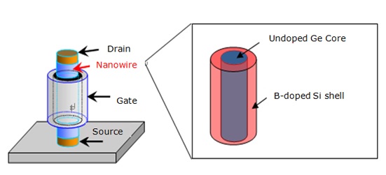
Figure 1: Schematic of a vertical transistor and an expanded view of its core-shell nanowire part.
A research group led by Naoki Fukata, International Center for Materials Nanoarchitectonics, National Institute for Materials Science (NIMS), and a research group at Georgia Institute of Technology jointly developed a double-layered (core-shell) nanowire, consisting of a germanium (Ge) core and a silicon (Si) shell, which is a promising material for high-speed transistor channels. In addition, the groups verified that the Si layer, which was doped with impurities, and the Ge layer, which transports carriers, were not intermixed, and that carriers were generated in the Ge layer. These results suggest that the new nanowire may effectively suppress the impurity scattering, which had been a problem with conventional nanowires, thereby taking a major step toward the realization of a next-generation high-speed transistor.
Regarding the development of two-dimensional metal-oxide-semiconductor field-effect transistors (MOSFETs), which are now widely used, it was pointed out that efforts to miniaturize the MOSFET using conventional technology had reached the limit. To deal with this issue, the development of a three-dimensional vertical transistor, instead of a two-dimensional transistor, was proposed as a new approach to realize high integration (Figure 1). The use of semiconducting nanowires as channels—the most vital part of the 3-D transistor—had been suggested. However, there was a problem with this method: in nanowires with a diameter of less than 20 nm, impurities doped into the nanowires to generate carriers caused the carriers to scatter, which in turn decreased their mobility.
By developing nanowires consisting of a Ge core and a Si shell, the research groups succeeded in creating high mobility channels capable of separating impurity-doped regions from carrier transport regions, thereby suppressing impurity scattering. The groups also successfully verified the performance of the channels.
Carriers are generated in the Si shell of the nanowires, introduced into the Ge core. Because carrier mobility is higher in the Ge layer than in the Si layer, this nanowire structure increases carrier mobility. In addition, this structure also suppresses the effect of surface scattering, which occurs commonly in conventional nanowires. Furthermore, the groups verified that the concentration of carriers can be controlled by the amount of doping.
Because the creation of the core-shell structure requires only simple materials—silicon and germanium, it is feasible to manufacture the nanowires at low cost. In future studies, we plan to actually construct devices employing the core-shell structure, and assess their potential as high-speed devices by evaluating their characteristics and performance.
This study was conducted as a part of the research project titled “Control of carrier transport by selective doping of core-shell heterojunction nanowires” (Naoki Fukata, principal investigator) funded by the Japan Society for the Promotion of Science’s Grants-in-Aid for Scientific Research (A) program, and the NIMS 3rd Mid-Term Program project on chemical nanotechnology.
(This study was published in ACS NANO on Nov.11,2015: Naoki Fukata, Mingke Yu, Wipakorn Jevasuwan, Toshiaki Takei, Yoshio Bando, Wenzhuo Wu, and Zhong Lin Wang: Clear experimental demonstration of hole gas accumulation in Ge/Si core-shell nanowires[DOI: 10.1021/acsnano.5b05394])

Figure 2. An EDX (energy-dispersive X-ray spectroscopy) image of a Ge/Si core-shell nanowire created by a CVD process. (Red, Si area; blue, Ge area.)