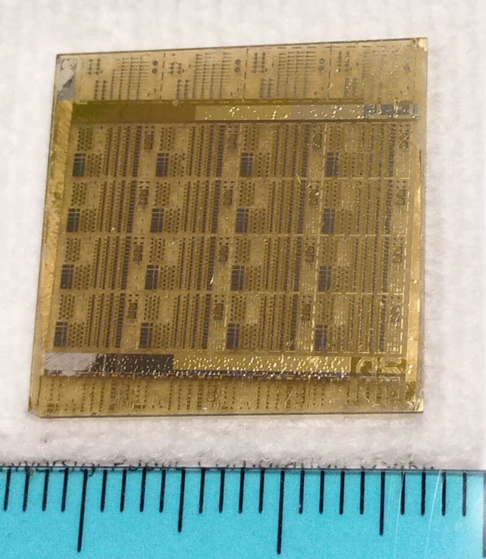
Gallium nitride (GaN) transistor on a diamond substrate: The integration of a 3C-SiC layer between GaN and diamond significantly reduces thermal resistance at the interface and improves heat dissipation, allowing for better performance.
Researchers at Osaka Metropolitan University are proving that diamonds are so much more than just a girl’s best friend. Their groundbreaking research focuses on gallium nitride (GaN) transistors, which are high-power, high-frequency semiconductor devices used in mobile data and satellite communication systems. With the increasing miniaturization of semiconductor devices, problems arise such as increases in power density and heat generation that can affect the performance, reliability, and lifetime of these devices. Therefore, effective thermal management is crucial. Diamond, which has the highest thermal conductivity of all natural materials, is an ideal substrate material but has not yet been put to practical use due to the difficulties of bonding diamond to GaN elements.
A research team led by Associate Professor Jianbo Liang and Professor Naoteru Shigekawa of the Graduate School of Engineering at Osaka Metropolitan University has successfully fabricated GaN High Electron Mobility Transistors using diamond as a substrate. This novel technology has more than twice the heat dissipation performance of transistors of the same shape fabricated on a silicon carbide (SiC) substrate. To maximize the high thermal conductivity of diamond, the researchers integrated a 3C-SiC layer, a cubic polytype of silicon carbide, between GaN and diamond. This technique significantly reduces the thermal resistance of the interface and improves heat dissipation.
“This new technology has the potential to significantly reduce CO2 emissions and potentially revolutionize the development of power and radio frequency electronics with improved thermal management capabilities,” said Professor Liang.
The results of this research were published in Small.
###
About OMU
Osaka Metropolitan University is the third largest public university in Japan, formed by a merger between Osaka City University and Osaka Prefecture University in 2022. OMU upholds "Convergence of Knowledge" through 11 undergraduate schools, a college, and 15 graduate schools. For more research news visit https://www.omu.ac.jp/en/ or follow us on Twitter: @OsakaMetUniv_en, or Facebook.