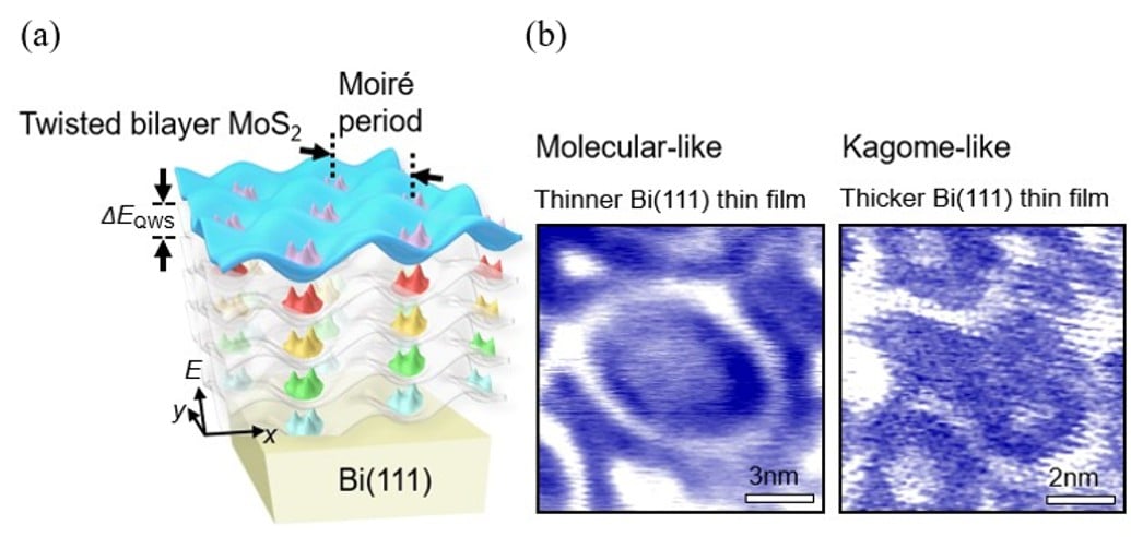
(a) Schematic diagram of twisted bilayer MoS2 (tb-MoS2) forming periodic moiré patterns stacked on top of thickness-dependent semimetal Bi quantum well states (∆E_QWS). The twisted bilayer MoS2 and the Bi metal thin film provide electronic confinement effects parallel and perpendicular to the film plane, respectively, jointly regulating the spatial arrangement of electrons.
(b) Thickness control of the Bi semimetal thin film gives rise to distinctly different electron spatial arrangement patterns:
(left) In thinner Bi semimetal films, molecular-like electron arrangement behavior.
(right) In thicker Bi semimetal films, Kagome-like electron arrangement behavior.
A recent study published in Nature Communications demonstrates precise control over electron spatial arrangement in two directions simultaneously - without any applied voltage - through interface engineering between semimetal bismuth (Bi) thin films and two-dimensional semiconductor MoS₂.
Researchers found that in the horizontal direction, the Moiré potential generated by small-angle twisted bilayer MoS₂ confines electrons to specific sites; in the vertical direction, tuning the bismuth film thickness to modulate the electron effective mass, enabling switching between two distinct configurations - thinner films favor electron clustering into a trimer (molecular-like bonding) arrangement, while thicker films drive electrons apart into a periodic Kagome-like configuration.
Requiring no external voltage to induce electron confinement, this material system offers a critical foundation for developing charge qubits and ultra-low-power devices, potentially opening new design pathways for next-generation quantum computing and energy-efficient semiconductor chips.
In this work, the team of Distinguished Professor Ya-Ping Chiu in the Department of Physics at National Taiwan University was responsible for the core atomic-scale experimental measurements and analysis.
Director and Distinguished Research Fellow Ching-Ming Wei of the Institute of Atomic and Molecular Sciences, Academia Sinica, together with the team of Professor Jyh-Pin Chou of the Graduate School of Advanced Technology, National Taiwan University, provided crucial support with theoretical calculations. The R&D team at Taiwan Semiconductor Manufacturing Company (TSMC) supplied high-quality semiconductor samples.
“Bidirectional, gate-free manipulation of quantum electronic states offers a materials foundation for next-generation quantum computing and energy-efficient semiconductor technologies,” says co-corresponding author Prof. Ya-Ping Chiu.
Prof. Ya-Ping Chiu's email address: [email protected]