Tokyo, Japan – 3D integrated circuits are a key part of improving the efficiency of electronics to meet the considerable demands of consumers. They are constantly being developed, but translating theoretical findings into actual devices is not easy. Now, a new design by a research team from Japan can turn these theories into reality.
In a study recently published for the VLSI Symposium 2023, researchers from Institute of Industrial Science, The University of Tokyo have reported a deposition process for nanosheet oxide semiconductor. The oxide semiconductor resulting from this process has high carrier mobility and reliability in transistors.
3D integrated circuits are made up of multiple layers that each play a role in the overall function. Oxide semiconductors are attracting a lot of attention as materials for various circuit components because they can be processed at low temperature, while still having high carrier mobility and low charge leakage, and are able to withstand high voltages.
There are also advantages to using oxides rather than metals in processes where electrodes may be exposed to oxygen during the integration process and become oxidized.
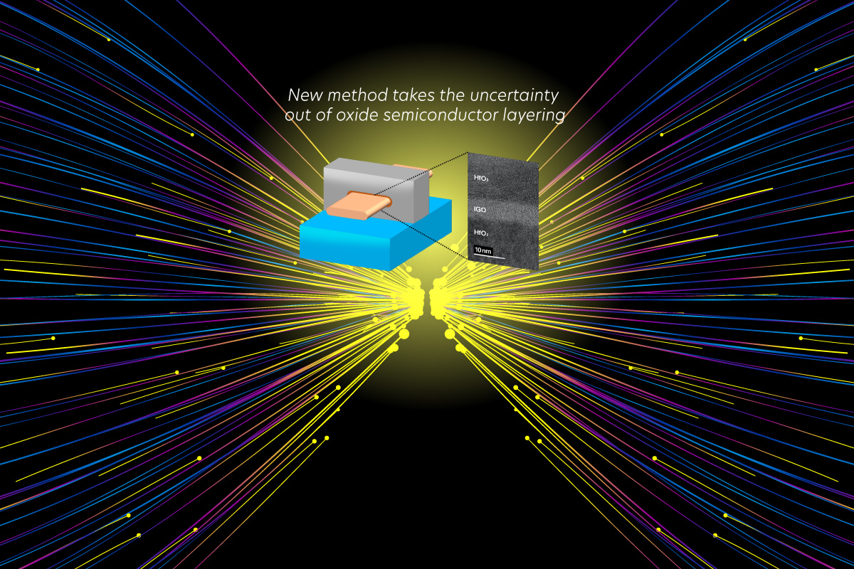
However, developing the processes needed to reliably deposit very thin layers of oxide semiconductor materials in the manufacture of devices is challenging and has not been fully established to date. Recently, the researchers have reported an atomic layer deposition (ALD) technique that produces layers appropriate for large-scale integration.
“Using our process, we carried out a systematic study of field effect transistors (FETs) to establish their limitations and optimize their properties,” explains lead author of the study, Kaito Hikake. FETs control the current flow in a semiconductor. “We tuned the ratio of the components and adjusted the preparation conditions and our findings led to the development of a multi-gate nanosheet FET for normally-off operation and high reliability.”
The findings revealed that a FET made from the chosen oxide semiconductor by ALD had the best performance. The multi-gate nanosheet FET is believed to be the first to combine high carrier mobility and reliability characteristics with normally-off operation.
“In rapidly moving areas such as electronics, it is important to translate proof of concept findings into industrially relevant processes,” says Masaharu Kobayashi, senior author. “We believe that our study provides a robust technique that can be used to produce devices that meet the market’s need for manufacturable 3D integrated circuits with high function.”
The findings in this study have provided a solution to one of the big obstacles in the manufacturing of electronic devices with semiconductors. Hopefully, this will bring more designs of electronics with high functionality to actual products.
###
The article, “A Nanosheet Oxide Semiconductor FET Using ALD InGaOx Channel and InSnOx Electrode with Normally-off Operation, High Mobility and Reliability for 3D Integrated Devices”, was published for the VLSI Symposium 2023.
About Institute of Industrial Sciene, The University of Tokyo
The Institute of Industrial Science, The University of Tokyo (UTokyo-IIS) is one of the largest university-attached research institutes in Japan. UTokyo-IIS is comprised of over 120 research laboratories—each headed by a faculty member—and has over 1,200 members (approximately 400 staff and 800 students) actively engaged in education and research. Its activities cover almost all areas of engineering. Since its foundation in 1949, UTokyo-IIS has worked to bridge the huge gaps that exist between academic disciplines and real-world applications.
Advertisement