
Prof. Kyung-In Jang, DGIST & Integrated Master’s and Ph.D. student Jeongdae Ha,
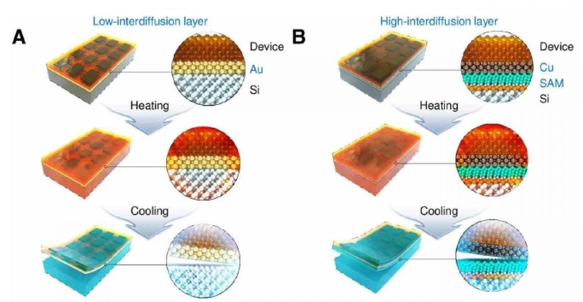
(A) Schematic illustration of the process for dry transfer printing depending on the atomic diffusion level of the material with a high CTE. The process is classified into a low-interdiffusion layer (Au) and (B) a high-interdiffusion layer (Cu), necessitating an antiatomic diffusion layer.
New technology that enables more efficient and effective transfer printing for electronic devices has been developed by researchers at the Daegu Gyeongbuk Institute of Science and Technology (DGIST) in Korea.
Published in the journal Science Advances, the technique could improve the manufacturing of precision devices such as biosensors and wearable devices.
“Our research team is the first to develop an instant dry transfer printing technology that can be used on both a small and large scale without the need for expensive equipment,” explains Seungkyoung Heo, one of the lead authors of the DGIST study.
Transfer printing takes functional elements from one material and applies them to another material. The method can produce flexible and stretchable electronic devices used in a wide variety of applications, such as wireless communications systems, wearable health monitors and flexible electronic displays.
The most common manufacturing technique, called wet transfer printing, has a number of drawbacks that limit its use. These include limited accuracy, long processing times and displacement or distortion of the device caused by the movement of fluid during the printing process. In recent years, alternative dry transfer printing methods have been developed, but they require specific conditions or expensive equipment such as lasers, so they have not been used widely.
The innovative printing technique developed by the DGIST researchers is the most versatile and scalable dry transfer method produced so far. Importantly, the technique can be used by small-scale research facilities without access to conventional dry transfer printing equipment.
The novel printing technique makes use of the fact that different materials expand at different rates when heated. By laying the device to be printed onto the surface to which it will be attached and then increasing the temperature, the method causes thermal stress which creates cracks between the layers. This allows the layers to be separated successfully after printing, ensuring reliable and instant release of the device.
In this study, the researchers demonstrated the high versatility of this technique by making an electrocardiogram sensor, a gas sensor, an optogenetic probe, and a wireless power transmission antenna.
Lab analysis confirmed the novel printing technique is more accurate and faster than conventional wet transfer printing methods. The new dry transfer printing method takes just a few seconds and maintains the original shape and structure of the device after the release process, unlike wet transfer printing which is slower and can cause wrinkling. The dry printing technique can also be scaled up to accommodate many different pattern sizes and shapes, and it can be integrated with other widely used printing tools such as thermal release tape.
It also has the advantage of being able to precisely transfer devices with complex structures, which could improve productivity in the precision device industry and high-tech industries.
“We now plan to further optimize the technology by integrating it into many of the biosensors, wireless power transfer systems, and stretchable devices being studied in our laboratory,” says Jeongdae Ha, another lead author of the study from DGIST.