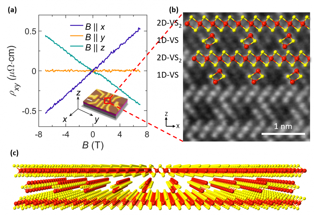
Discovery of a new superlattice structure exhibiting the anisotropic Hall effect. (a) Anisotropic Hall effect. (b) Scanning transmission electron microscopy (STEM) cross sectional image of 2D-VS2/1D-VS superlattice structure. (c) Schematic model of the 2D/1D hybrid superlattice.
Researchers from Osaka University and collaborating partners use routine nanofabrication procedures to prepare a revolutionary metal superlattice. This development will enhance the utility of microelectronics in common technologies
Osaka, Japan – Breakthroughs in modern microelectronics depend on understanding and manipulating the movement of electrons in metal. Reducing the thickness of metal sheets to the order of nanometers can enable exquisite control over how the metal's electrons move. In so doing, one can impart properties that aren't seen in bulk metals, such as ultrafast conduction of electricity. Now, researchers from Osaka University and collaborating partners have synthesized a novel class of nanostructured superlattices. This study enables an unusually high degree of control over the movement of electrons within metal semiconductors, which promises to enhance the functionality of everyday technologies.
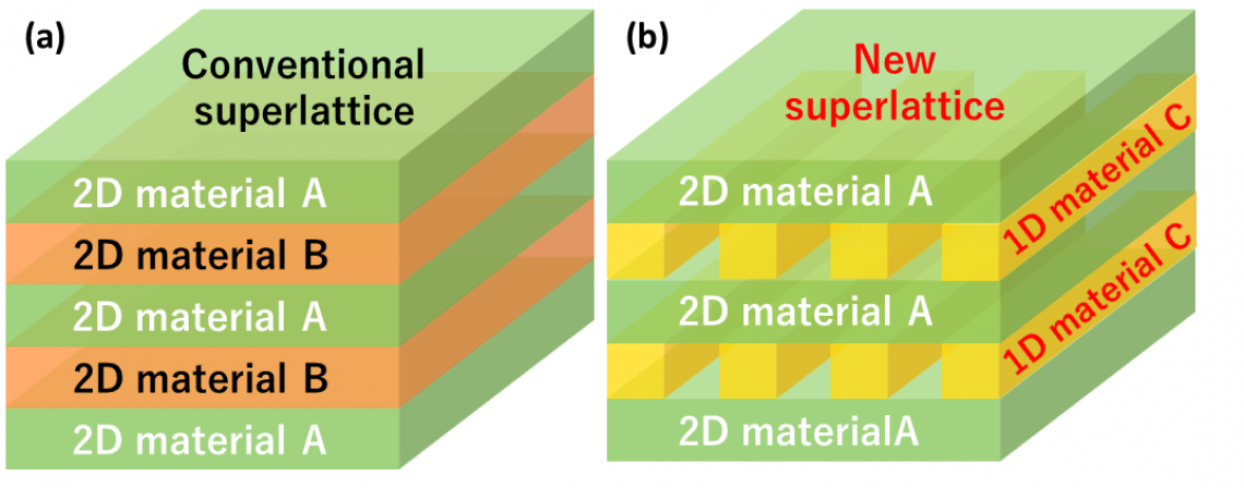
Precisely tuning the architecture of metal nanosheets, and thus facilitating advanced microelectronics functionalities, remains an ongoing line of work worldwide. In fact, several Nobel prizes have been awarded on this topic. Researchers conventionally synthesize nanostructured superlattices—regularly alternating layers of metals, sandwiched together—from materials of the same dimension; for example, sandwiched 2D sheets. A key aspect of the present researchers' work is its facile fabrication of hetero-dimensional superlattices; for example, 1D nanoparticle chains sandwiched within 2D nanosheets.
"Nanoscale hetero-dimensional superlattices are typically challenging to prepare, but can exhibit valuable physical properties, such as anisotropic electrical conductivity," explains Yung-Chang Lin, senior author. "We developed a versatile means of preparing such structures, and in so doing we will inspire synthesis of a wide range of custom superstructures."
Fig. 2. (a) Conventional superlattice structure model consisting of different 2D materials. (b) Newly discovered superlattice structure model consisting of two-dimensional (film-like) and one-dimensional (chain-like) materials.
The researchers used chemical vapor deposition—a common nanofabrication technique in industry—to prepare vanadium-based superlattices. These magnetic semiconductors exhibit what is known as an anisotropic anomalous Hall effect (AHE): meaning directionally focused charge accumulation under in-plane magnetic field conditions (in which the conventional Hall effect isn't observed). Usually, the AHE is observed only at ultra-low temperatures. In the present research, the AHE was observed at room temperature and higher, up to around at least the boiling point of water. Generation of the AHE at practical temperatures will facilitate its use in everyday technologies.
"A key promise of nanotechnology is its provision of functionalities that you can't get from bulk materials," states Lin. "Our demonstration of an unconventional anomalous Hall effect at room temperature and above opens up a wealth of possibilities for future semiconductor technology, all accessible by conventional nanofabrication processes."
The present work will help improve the density of data storage, the efficiency of lighting, and the speed of electronic devices. By precisely controlling the nanoscale architecture of metals that are commonly used in industry, researchers will fabricate uniquely versatile technology that surpasses the functionality of natural materials.
###
The article, "Heterodimensional superlattice with room-temperature anomalous Hall effect," was published in Nature at DOI: https://doi.org/10.1038/s41586-022-05031-2
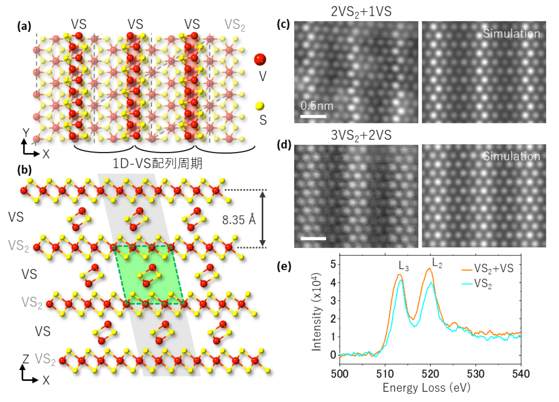
Fig. 3. (a) Atomic model of stacking structure of VS2-VS superlattice viewed from top. Red and yellow balls represent V and S atoms. (b) Atomic model of VS2-VS superlattice viewed from the side. The green rectangle is the unit cell of the superlattice. (c,d) STEM images of 2D-film/1D-chain/2D-film (VS2/VS/VS2) superlattice structure and 2D-film/1D-chain/2D-film/1D-chain/2D-film (VS2/VS/VS2/VS/VS2) superlattice structure and the corresponding simulated STEM images. (e) Electron energy-loss near edge fine structure of the L-edge of the V atom.


