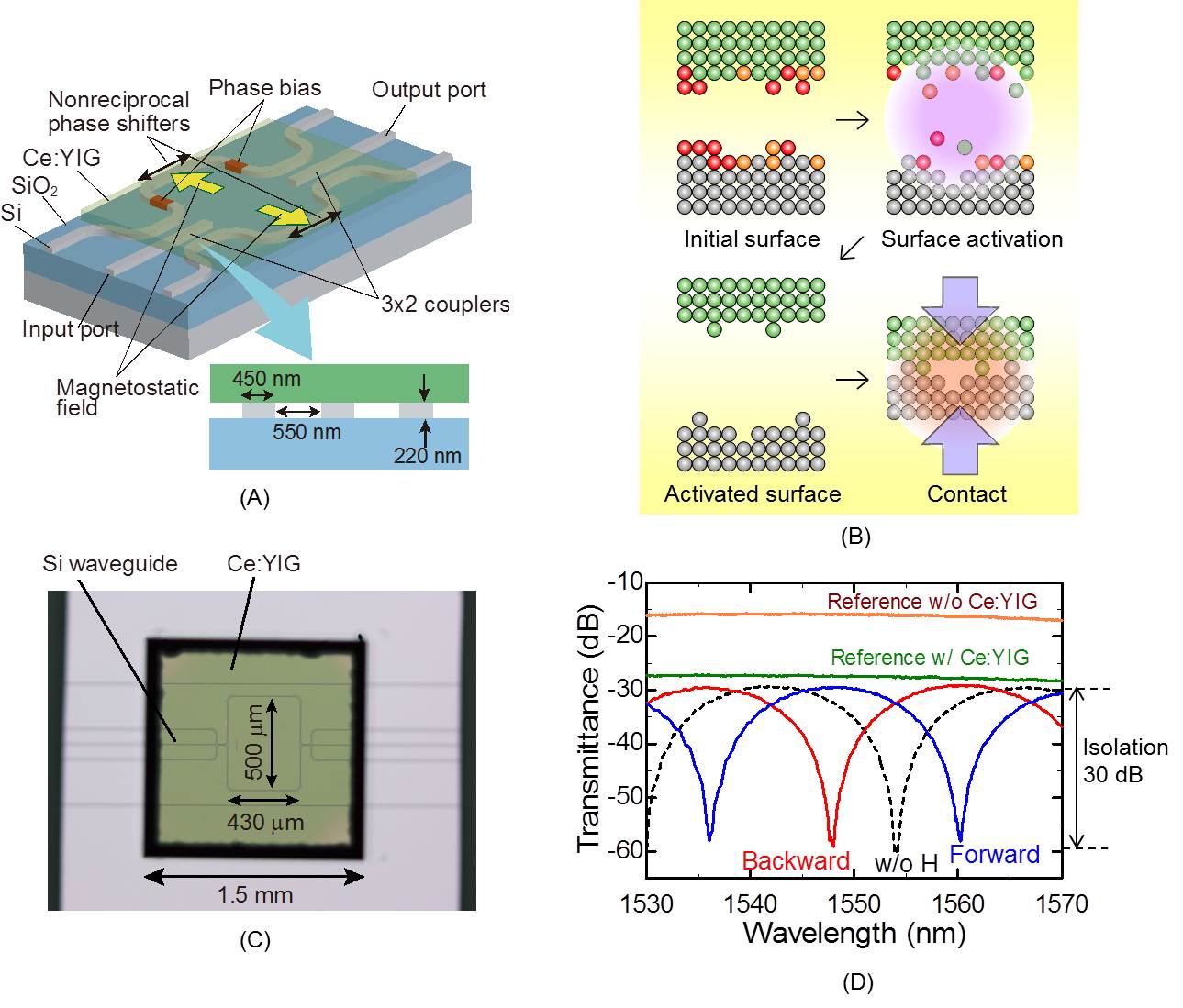
Figure caption: (A) Schematic illustration of an SOI waveguide optical isolator based on MZI, (B) Process of direct bonding technique, (C) Microscope image of a fabricated optical isolator, (D) Measured fiber-to-fiber transmittance of the fabricated optical isolator as a function of the wavelength.
As the recent demand for optical interconnections is increased, much attention has been paid to silicon photonics because of the small device footprint and CMOS compatible process. An optical isolator is essential for protecting optical active devices from reflected light even in short-distance transmission systems.
However, the bottleneck of integrated optical isolator lies in difficulty in growing magneto-optical garnet crystals on commonly used optical waveguide platforms such as silicon.
Yuya Shoji and Tetsuya Mizumoto of Tokyo Institute of Technology, approached the problem using a direct bonding technique which realizes direct contact of different materials. The authors have demonstrated the first optical isolator on silicon waveguide platforms.
In this paper published in Science and Technology of Advanced Materials, they describe the direct bonding, design of the waveguide isolator, and recent progress on a silicon isolator with an optical isolation of 30 dB and a four port optical circulator. They also introduce approaches done by other research groups in the paper.
Compared to the state-of-the-art deposition approach, the bonding technique is advantageous because a single-crystalline magneto-optical garnet having a large magneto-optical effect can be used.
Contact authors:
Yuya Shoji and Tetsuya Mizumoto
Department of Electrical and Electronic Engineering, Tokyo Institute of Technology, 2-12-1 Ookayama, Meguro-ku, Tokyo 152-8552, Japan
E-mail: [email protected] and [email protected]