□ The team, led by Professor Jiwoong Yang from the Department of Energy Engineering at DGIST (President Kuk Yang), and in collaboration with the team led by Professor Jungwon Park from the School of Chemical and Biological Engineering at Seoul National University (President Ryu Hong-lim), determined the moisture- (water-) induced degradation[1] mechanism of semiconductor nanocrystal quantum dots. The joint research team developed the next-generation imaging platform for in-situ liquid-phase transmission electron microscopy (TEM), which can be used to reveal the reaction intermediates and atomic unit reaction paths that exist in the degradation process, thereby taking one step closer to the commercialization of nanocrystal quantum dots.
□ Semiconductor nanocrystal quantum dots find extensive applications in diverse fields such as bioimaging, optoelectronic devices, and catalysts due to their advantageous features, including size and shape-dependent band gaps[2], high lamp efficiency, and narrow full width at half maximum[3]. However, they also exhibit drawbacks such as reduced stability when exposed to moisture and oxygen compared to bulk semiconductor crystals. As a result, numerous studies are underway to create semiconductor nanocrystal quantum dots with enhanced stability against the impact of moisture and oxygen. Nevertheless, the development process faces challenges because the specific "degradation" mechanism, which causes deterioration of their properties due to external factors, has not been fully explained.
□ Studies have been conducted using spectrometry, X-ray scattering, and diffraction analysis to identify the degradation mechanism; however, these methods could only identify the changes in optical and physical properties of nanocrystals in the moisture-induced degradation process, providing only average information on structural changes. Moreover, there are limitations in revealing the existence of various atomic unit reaction patterns and reaction intermediates that may occur in individual nanoparticles, as it is difficult to determine the structural change mechanism of individual nanocrystals.
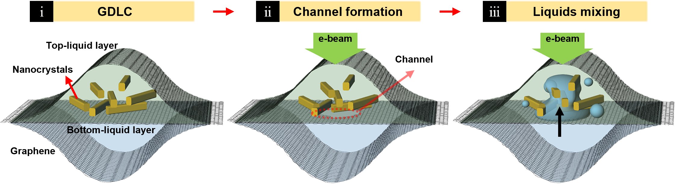
□ Accordingly, Professor Jiwoong Yang's team at DGIST devised a method using in-situ liquid-phase TEM, enabling the observation of the reaction process of individual nanoparticles in real-time. In particular, liquid cells capable of both reaction control and real-time ultra-high-resolution imaging were needed to identify the moisture-induced degradation mechanism. For this purpose, the team developed “graphene-based next-generation liquid cells” that possess both functions. These next-generation liquid cells are designed to control the mixture of two different liquids through extremely thin graphene membranes.
□ Furthermore, research was conducted to reveal the degradation mechanism using “cadmium sulfide (CdS),” which is a well-known crystallization method for nanocrystal quantum dots. The results revealed that “cadmium sulfide (CdS)” semiconductor nanocrystals undergo decomposition by forming amorphous intermediates comprised of Cd(OH)x during the degradation process. Moreover, the presence of this amorphous intermediate leads to an irregularly shaped crystal surface structure in the middle of the reaction, which is different from the previously studied degradation mechanism of metal nanocrystals. This confirmed the importance of protecting the surface of semiconductor nanocrystals, as the moisture-induced structural degradation of semiconductor nanocrystals is irreversible and initiates from the surface.
□ "Moisture-induced degradation has been a key factor causing difficulties in commercializing semiconductor nanocrystal quantum dots," stated DGIST Professor Jiwoong Yang. "The degradation mechanism revealed in this study is expected to significantly contribute to the future development of quantum materials."
□ Additionally, this research received support from the Samsung Future Technology Incubation Program, and the research findings were published in the online edition of the esteemed nanoscience journal "ACS Nano" in July.
Correspondence Author Email Address : [email protected]
[1] Degradation: A phenomenon in which the chemical and physical properties of an insulator deteriorate due to external or internal effects.
[2] Band gap: This refers to the energy region in semiconductors and insulators where the density of electron states between the valence band and the conduction band becomes zero.
[3] Full width at half maximum: This represents the width of a line shape at half of its maximum amplitude, as depicted by the bump on a curve.