
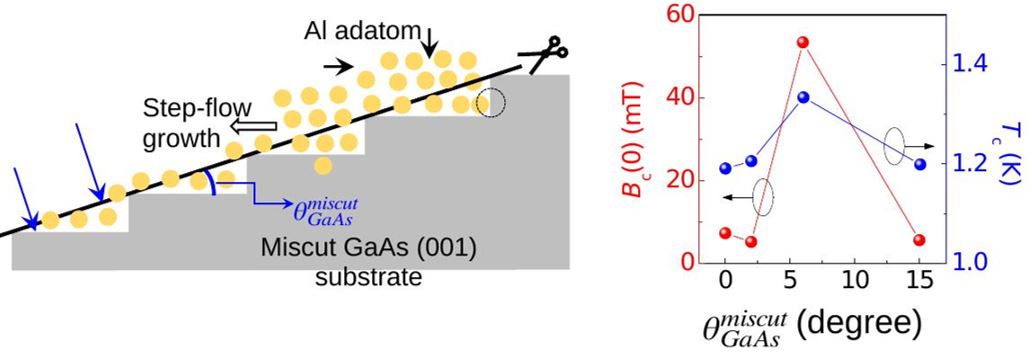
Left panel: An Al nanofilm grown on GaAs with a miscut angle. Right panel: Modulation of Tc, and Bc at different GaAs substrate miscuts.
Aluminum’s research and practical importance
Aluminum (Al) is one of the most important metallic elements because of its fundamental importance and practical device applications. In particular, Al thin films have attracted significant attention for their critical roles in heat sinks, interconnects, plasmonics, superconducting devices, and quantum computing. The superconducting critical temperature Tc , current Ic, and magnetic field Bc of an Al thin film are probably the most crucial physical quantities in the field of superconductivity and quantum computation.
Growing ultra-high-quality and wafer Al nanofilms
Given the significant global interest and research attention, researchers aim to prepare ultra-clean, wafer-scale aluminum superconductors by prioritizing high crystallinity, Tc, Ic, and Bc, while minimizing twin density, surface roughness, and normal-state sheet resistance.
To this end, an international team led by Professors Sheng-Di Lin and Shun-Tsung Lo at National Yang Ming Chiao Tung University (NYCU) and Chi-Te Liang at National Taiwan University (NTU), Taiwan work on growing wafer-scale Al nanofilms on GaAs substrate with different miscut angles by molecular beam epitaxy (MBE), a technique for preparing ultra-high-quality materials. The study is published in Small.
Tailoring grain architecture and superconductivity in aluminum
It is found that a 6° GaAs miscut angle modulates Tc, Ic, and Bc, by approximately 10%, 100%, and 1000%, respectively, compared to 40-nm-thick counterparts grown on 0°, 2°, and 15° miscut substrates. Although the twin density is also significantly reduced in this case, strain-induced crystallinity deterioration occurs, driving a transition from type-I to type-II-like superconducting behavior. Nevertheless, this simple approach using substrate-miscut strategy offers a glimpse of engineering MBE-grown Al grain boundaries, refining the crystallinity, and enhancing the superconductivity.
“Our work paves the way for controllably tailoring grain architecture and superconductivity in Al, with implications for both fundamental research and practical device applications,” says co-corresponding author Chi-Te Liang, Ph.D., professor of physics at National Taiwan University.
Prof. Chi-Te Liang's email address: [email protected]
Advertisement