


Researchers from Kanazawa University and AIST, in Japan, have demonstrated the world's first trench-type inversion-channel diamond MOSFET with normally-off operation.
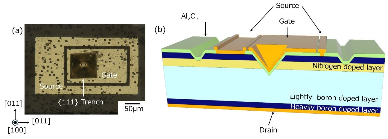
Figure 1. (a) Top view of a trench-type inversion-channel diamond MOSFET (b) Schematic cross-section of a trench-type inversion-channel diamond MOSFET
Adapted from Y. Nakamura, M. Nagai et al., Diamond and Related Materials (2026), CC BY 4.0.
In a joint study, Professor Norio Tokuda of the Advanced Research Center for Diamond Science and Technology, Kanazawa University; Yuto Nakamura, a doctoral student in the Division of Electrical, Information and Communication Engineering, Graduate School of Natural Science and Technology, Kanazawa University; Dr. Masatsugu Nagai of the Diamond Device Research Team, Advanced Power Electronics Research Center, National Institute of Advanced Industrial Science and Technology (AIST); and their colleagues have successfully demonstrated the operation of a trench-type (*1) inversion-channel diamond MOSFET (*2) for the first time in the world.
This achievement represents a direct leap from the previously demonstrated lateral-type (*3) inversion-channel diamond MOSFET to the trench-type structure, which offers the lowest power loss, without passing through the planar type (*4). Moreover, because both the planar type and the trench type are vertical structures, this achievement also represents the world’s first demonstration of a vertical diamond MOSFET incorporating an inversion channel.
As efforts toward achieving carbon neutrality advance, energy-saving technologies are becoming increasingly important. Owing to its exceptional physical properties, diamond is expected to serve as the “ultimate semiconductor material,” with the potential to enable ultralow-loss power devices. In particular, the trench-type diamond MOSFET is regarded as one of the ultimate forms of low-loss power devices, and extensive research and development efforts have been devoted to its practical realization. However, owing to their operating principles, trench-type diamond MOSFETs reported to date have faced challenges in reliably achieving normally-off (*5) operation, which is required for power devices.
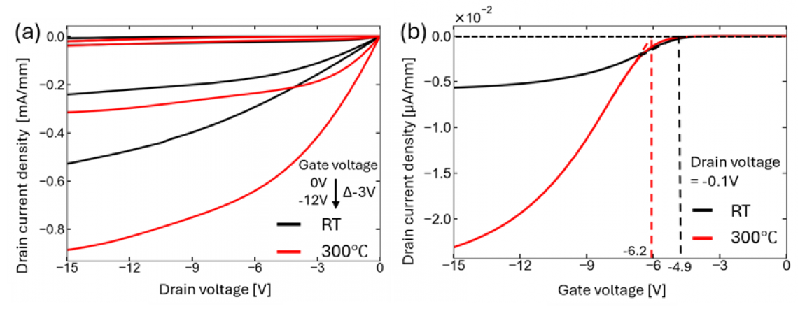
To address this challenge, the research team combined a fabrication technology for lateral-type inversion-channel diamond MOSFETs, which can inherently provide normally-off characteristics, with a proprietary crystal-anisotropic (*6) diamond etching technology that utilizes the carbon solid-solution reaction (*7) into nickel (Ni) in a water-vapor atmosphere. By combining these technologies, the team fabricated a trench-type inversion-channel diamond MOSFET (Fig. 1) and successfully demonstrated its operation (Fig.2). The fabricated device exhibited clear FET characteristics (*8) not only at room temperature but also at 300 ℃, confirming that it can achieve normally-off operation, an important feature for ensuring the safety of power devices.
Building on the knowledge gained through this study, the team will further optimize the device structure to achieve even lower power loss. In the future, these devices are expected to contribute to carbon neutrality through their application in electric vehicles (EVs) and power grids.
The results of this study were published in Diamond and Related Materials on September 10, 2026.
Figure 2. Electrical characteristics of a trench-type inversion-channel diamond MOSFET at room temperature and 300 ℃: (a) Drain current density–drain voltage characteristics, (b) Drain current–gate voltage characteristics
Adapted from Y. Nakamura, M. Nagai et al., Diamond and Related Materials (2026), CC BY 4.0
Glossary
*1 Trench-type
One type of MOSFET structure in which a groove (trench) or recess is formed in a semiconductor and its sidewall is used as a path for electric current that can be opened and closed (channel). A MOSFET is a field-effect transistor with a metal-oxide-semiconductor structure and is a device that controls the on and off states of current by means of a voltage applied to the gate. The trench-type is classified as a “vertical” structure, in which current flows in the vertical direction through the substrate. By forming the channel on the trench sidewall, in the vertical direction, the channel density per unit area can be increased. In addition, a loss component known as “JFET resistance” does not arise. As a result, the on-resistance can be kept low, and the trench-type is considered the MOSFET structure most advantageous for reducing power loss. The term “trench” originally means a “groove”; however, in the semiconductor field, recess-shaped structures such as this are also conventionally referred to as trenches.
*2 Inversion-channel diamond MOSFET
A diamond device that is a type of MOSFET (*1) and uses an inversion-layer as its channel. An inversion-layer is a conductive layer formed when carriers, which are present in small numbers in the semiconductor directly beneath the gate and serve as the carriers of electric current, are gathered at the semiconductor surface by a gate voltage. This is a common operating principle of MOSFETs, and no current flows when no voltage is applied to the gate. This characteristic is referred to below as “normally-off” (*5).
*3 Lateral-type
A MOSFET structure in which current flows in the horizontal direction through the substrate. Although the structure is simple and easy to fabricate, designing the device to withstand high voltages causes the resistance per unit device area (on-resistance) to increase sharply. For this reason, it is not suitable for power devices that handle high voltages and high power.
*4 Planar-type
One type of “vertical” MOSFET structure, in which current flows in the vertical direction through the substrate and the channel is formed on the flat substrate surface rather than on the trench sidewall. It can handle higher voltages and higher power than the lateral-type (*3). Compared with the trench-type (*1), however, a loss component known as “JFET resistance” arises because of its structure. In addition, because the channel-forming region is limited to the substrate surface, it is difficult to increase the channel density. These two factors increase the on-resistance, resulting in lower energy efficiency.
*5 Normally-off
A characteristic in which no current flows when no voltage is applied to the gate, and current flows only after a voltage is applied. In contrast, a characteristic in which current flows even when no voltage is applied is referred to as “normally-on.” Normally-off operation is considered an essential characteristic for power devices because it allows the current to be automatically interrupted and the system to be brought to a safe stop in the event of a power failure or system malfunction, thereby providing fail-safe operation.
*6 Crystal-anisotropy
The property whereby a structure in which atoms are arranged in an orderly manner (a crystal) exhibits different properties depending on its direction (crystallographic orientation). In this study, it refers to the property whereby etching becomes extremely slow on the diamond {111} planes. Because of this property, other planes are preferentially removed and the {111} planes remain as sidewalls, making it possible to form trenches with {111} sidewalls.
*7 Carbon solid-solution reaction
The phenomenon in which one solid dissolves into the interior of another solid at the atomic level is referred to as a “solid-solution.” A carbon solid-solution reaction refers to a reaction in which carbon dissolves into another solid, which in this study is nickel. In this study, this reaction was used in a high-temperature water-vapor atmosphere to dissolve carbon from the diamond surface into nickel, thereby partially removing (etching) the diamond without using chemicals or plasma.
*8 FET characteristics
Electrical characteristics indicating that a field-effect transistor (FET) is operating properly. Specifically, these characteristics include the ability to control the magnitude of the current flowing through the device (drain current) by means of a voltage applied to the gate, as well as an increase in the drain current with increasing drain voltage, followed by saturation above a certain voltage.
Advertisement