The newly-fabricated EDL transistor with graphene oxide (GO) made by WPI-MANA researchers allows fine tuning of band gaps in the GO, meaning that conductivity, as well as magnetic and optical properties, can be carefully controlled.
Super-strong graphene oxide (GO) sheets are useful for ultrathin, flexible nano-electronic devices, and display unique properties including photoluminescence and room temperature ferromagnetism. Tsuchiya, Terabe and Aono at Japan's World Premier International Center for Materials Nanoarchitectonics (WPI-MANA) are developing novel techniques that allow them to fine tune the physical properties of GO, such as conductivity, within working components.
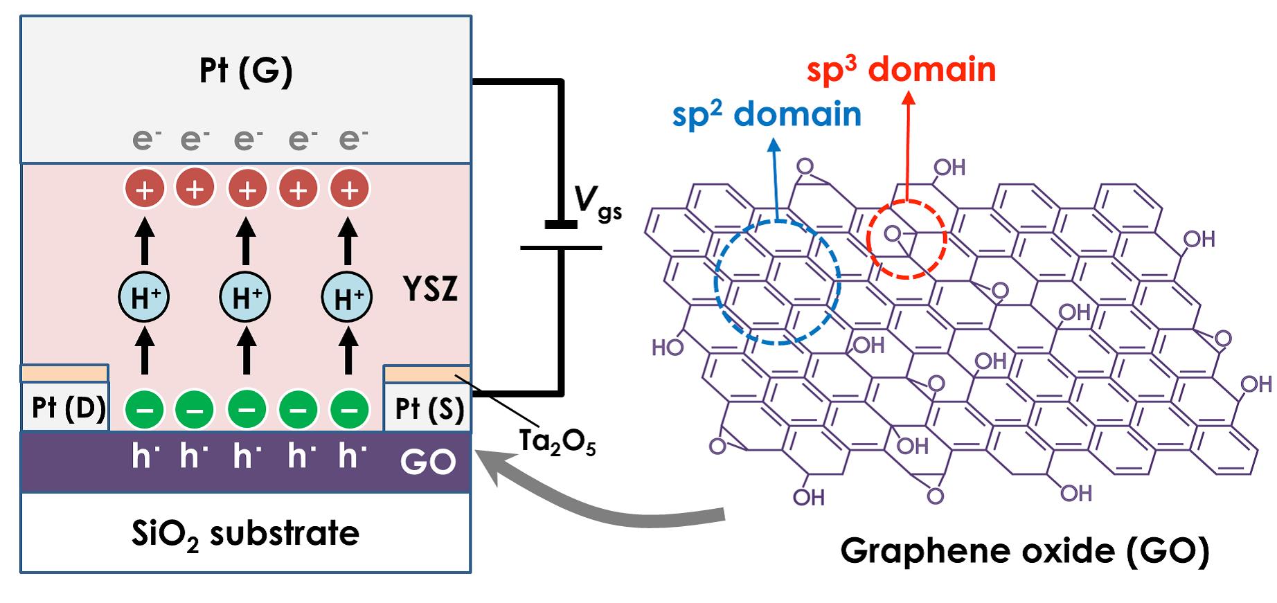
The conductivity of GO is lower than graphene itself because of disruptions within its bonding structure. Specifically, the carbon atoms in GO exhibit a blurring of energy levels called sp2 or sp3 hybridizations. In ordinary GO, bonding in the sp2 level is disrupted, and under severe disruption the GO becomes an insulator rather than a conductor. Highly-reduced GO (rGO), with lower oxygen levels, has a near-perfect hexagonal lattice structure with strong bonds and high conductivity.
By adjusting the percentages of sp2 and sp3 domains in GO, Terabe and his team have gained the ability to fine tune band gaps and therefore control conductivity. Current methods of controlling bandgaps in GO are chemically-based, expensive, and cannot be used within electronic components themselves.
Now, the team have achieved non-volatile tuning of bandgaps in multi-layered GO within an all-solid-state electric double layer transistor (EDLT). The EDLT comprised GO on a silica glass substrate gated by a zirconia proton conductor. The team triggered a reversible electrochemical reduction and oxidation (redox) reaction at the GO/zirconia interface by applying a dc voltage. This in turn caused proton migration from GO through the zirconia (see image).
The redox reaction created rGO, and caused a fivefold increase in current in the transistor.
The rGO retained conductivity for more than one month without further voltage application. Compared with field-effect transistors, the new EDLT uses far less voltage to switch between on and off phases, meaning it is far cheaper to use. This new method for fine tuning conductivity could lead to control over optical and magnetic properties of components, with far-reaching applications.
Contact Information
International Center of Materials Nanoarchitectonics (MANA)
National Institute for Materials Science
1-1 Namiki Tsukuba, Ibaraki 305-0044 JAPAN
Phone: +81-29-860-4710
E-mail: [email protected]
About MANA
http://www.nims.go.jp/mana/
In Situ Bandgap Tuning of Graphene Oxide Achieved by Electrochemical Bias
http://www.nims.go.jp/mana/research/highlight/vol10.html
Publisher
International Center for Materials Nanoarchitectonics (WPI-MANA)
Address: 1-1 Namiki, Tsukuba, Ibaraki 305-0044, Japan
URL: http://www.nims.go.jp/mana/